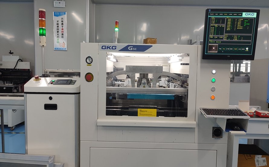
The SMT process includes adding solder paste, placing components, reflow soldering, wave soldering, cleaning, testing, and packaging.
Your Trusted Partner for Sensor PCB Fabrication
- Material: FR4, High-speed FR4, PTFE, Teflon, Radio Frequency, Microwave, Low Loss, Arlon, Rogers, Nelco/Taconic, Isola, Panasonic, and more.
- Technologies: Impedance control tolerance +/- 5%, PTFE+FR4 Hybrid, Ceramic+FR4 Hybrid.
- Material Thickness: 0.1-6.0mm.
- Copper Thickness: 1/3oz to 5oz.
- Min Trace Width/Space: 2mil (0.05mm).
- Min Drill Size: 3mil (0.1mm).
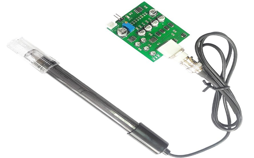
A Sensor PCB is a printed circuit board that integrates sensors and components into one unit. These boards can detect temperature, pressure, light, and object speed, with collected data being converted into electrical signals and processed by the chip. As the core of sensor systems, Sensor PCBs enable electronic devices to monitor their surroundings, with data being transmitted for operator analysis and decision-making.
Get a free quote now!
What are Sensor PCBs?

Get a free quote now!
Sensor PCBs integrate environmental sensors and components into a single circuit board, equipped with multiple communication ports to support various sensor types. Sensor PCBs detect environmental data and transmit it in the form of electrical signals. These boards can work with development boards to create monitoring systems applied across different sectors.
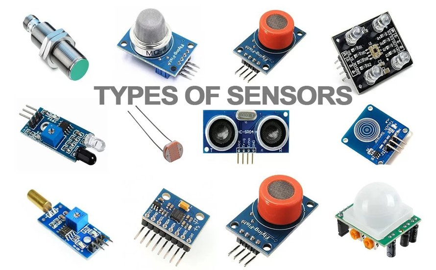
Types of Sensors Integrated into PCBs
Temperature Sensors
- Thermistors: Measure temperature by changing resistance.
- Thermocouples: Output voltage based on temperature difference, used in industrial control processes.
Pressure Sensors
- Piezoelectric Sensors: Convert pressure into electrical signals via the piezoelectric effect.
- Capacitive Sensors: Measure capacitance changes due to diaphragm deformation, often used in consumer electronics.

Motion Sensors
- Accelerometers: Measure acceleration forces, aiding orientation in smartphones.
- Gyroscopes: Detect rotational motion, crucial in vehicle navigation systems and drones.
Light Sensors
- Photodiodes: Convert light into electric currents, measuring light intensity.
- Phototransistors: Sensitive light detectors used in security devices.
Humidity Sensors
- Capacitive Humidity Sensors: Measure humidity by changing capacitance in polymer films.
- Resistive Humidity Sensors: Detect humidity through resistance changes in conductive polymers.
Sensor PCBs offer flexibility for applications from home gadgets to industrial machinery, allowing for compact, efficient designs with enhanced functionality.
Design Considerations for Sensor PCBs
Designing a Sensor PCB requires addressing environmental challenges, including temperature, humidity, and chemicals. PCBs for outdoor use must resist water and extreme temperatures, while industrial versions must handle vibrations and mechanical stress. Each application demands specific design choices, including material selection. Popular materials include FR4 (good insulation and thermal resistance), CEM1 (cost-effective and heat-resistant), and high-frequency materials like Rogers or Teflon for signal transmission.
Sensor PCB Manufacturing Process
Schematic Design & Layout:
Drafting the connection points and functional elements.
Material Selection & Stack-up:
Layering copper with insulating substrates.
Photolithography:
Using UV light to imprint the circuit onto the substrate.
Layering & Lamination:
Applying high temperature and pressure to form a solid board.

Drilling & Plating:
Pre-drilling seating for components and vias.
Component Placement & Soldering:
Using SMT for compact designs and Through-Hole Technology for robust connections.
Inspection & Quality Control:
Conducting AOI and X-ray tests to ensure accuracy.
Functional Testing:
Simulating working conditions to check circuit integrity.
Finishing & Cutting:
Applying protective coatings and cutting the boards into units.
Rigorous quality control ensures sensor PCBs meet performance and endurance requirements.
Applications of Sensor PCBs
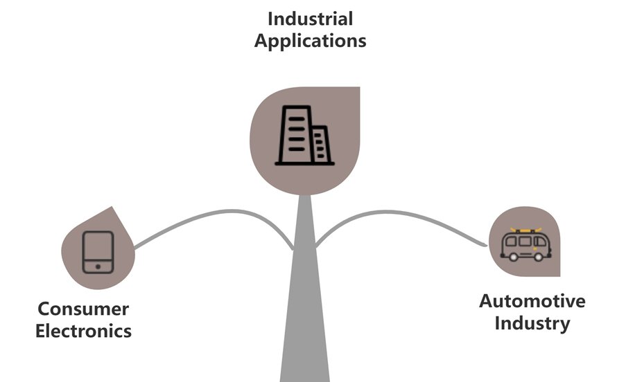
Sensor PCBs have transformed industries with new opportunities in technology. Key applications include:
Consumer Electronics
Used in smartphones and wearables for motion detection and health monitoring, enhancing user interactivity.
Industrial Applications
Used in automation and safety systems, ensuring operational efficiency and safety in industrial settings.
Automotive Industry
Integral to safety systems like collision detection and parking sensors, improving driving safety and performance.

Challenges in Sensor PCB Development
Miniaturization Challenges
Design complexity increases with tighter space constraints, requiring advanced thermal management.
Signal Integration and Interference
Multiple sensors can create signal interference, requiring shielding and optimized data layouts.
Environmental and Durability Challenges
Sensor PCBs must endure harsh environments, requiring materials resistant to water, heat, and mechanical damage.
ESPCBA: Your Expert in Sensor PCB Manufacturing
With 16 years of experience, ESPCBA excels in sensor PCB fabrication, offering:
High Reliability:
Our rigorous quality assurance ensures high-performance PCBs for your projects.
Competitive Pricing:
We offer fair pricing without sacrificing quality.
On-time Delivery:
We adhere to agreed timelines, ensuring prompt delivery.
Flexible Order Quantities:
We accommodate both small and medium-scale production needs.
Connect with us
Get an Instant Online Quote Today
Looking for reliable SMD assembly services? At ESPCBA, we’re your trusted partner for PCB fabrication, component sourcing, and electronic manufacturing. With over 16 years of experience, we’ve provided high-quality PCBs at competitive prices to over 1,000 customers worldwide. Our company is ISO9001:2015 certified and UL listed, and every product we deliver is 100% E-tested and inspected using AOI and X-ray to meet the highest standards. Get an instant quote from our sales team today, and let us handle the rest for you.
Frequently Asked Questions
A circuit board used in various sensor systems.
Copper, glass-fiber epoxy, and polyimide laminates.
Analog, Digital, and Mixed Signal sensor PCBs.
Sensors detect physical changes, converting them into electrical signals for processing.
Increased precision, compact size, efficiency, and reliability.
Temperature, pressure, flow, light, motion, current, voltage, and optical sensors.
Form factor, size, purpose, and electrical characteristics must be factored into the design.
Resistors, capacitors, diodes, transistors, switches, and connectors.
Consider materials, power supply design, grounding scheme, and sensor drive circuit.
Includes board cutting, drilling, copper etching, solder mask application, surface treatment, profiling, testing, and component assembly.
Thermal imaging is commonly used.
Sensors are typically mounted using SMT.
Using a specialized drill bit, either mechanical or laser.
Using electrical tests, AOI, functional testing, and more.
Layers are selected based on sensor requirements and optimized for minimal gaps.
Limited range, power requirements, high cost, and vulnerability.
Yes, it is moisture-resistant.
Look for experience, facility quality, and industry certifications like ISO9001 and UL.
Follow manufacturer instructions for installation.
Design flaws, poor manufacturing, and corrosion from environmental exposure.