Are defective solder joints compromising the reliability of your electronic products? In the world of PCB manufacturing, quality is paramount. One critical step that ensures high-quality results is Solder Paste Inspection (SPI).
We rely on SPI to verify key factors like solder paste volume, height, area, and alignment, catching defects early and preventing costly rework. By doing so, we ensure reliable electronic products that meet the increasing demands of miniaturization and complexity in modern electronics manufacturing.
As we explore the critical role of SPI in ensuring quality in Surface Mount Technology (SMT) manufacturing processes, we will examine its impact on the reliability and functionality of finished electronic products.
Key Takeaways
- Understanding the importance of Solder Paste Inspection (SPI) in SMT manufacturing.
- How SPI technology has evolved to meet modern electronics manufacturing demands.
- The role of SPI in reducing defect rates and improving production yields.
- Technical aspects of SPI and its implementation strategies.
- The impact of proper solder paste application on electronic product reliability.
Understanding Solder Paste Inspection in PCB Manufacturing
Solder Paste Inspection (SPI) is a crucial quality control measure in the PCB manufacturing process. We rely on SPI to ensure that solder paste is applied correctly to the printed circuit board (PCB) before component placement.
What is Solder Paste Inspection (SPI)?
SPI is an automated optical inspection technique that examines solder paste deposits on a PCB. It checks for issues such as insufficient or excessive solder paste volume, incorrect height, uneven area coverage, or misalignment. By detecting these defects early, SPI helps prevent downstream problems in the assembly process.
The Critical Role of SPI in Surface Mount Technology
In Surface Mount Technology (SMT), SPI plays a vital role in ensuring the quality and reliability of the final product. The SMT process involves applying solder paste to the PCB, placing components, and then reflowing the solder to create connections. SPI is the first critical checkpoint in this process, allowing manufacturers to identify and correct issues before they become major problems.
| Benefits of SPI | Description |
|---|---|
| Improved Quality | SPI ensures that solder paste is applied correctly, reducing the risk of defects |
| Increased Efficiency | By detecting issues early, SPI helps prevent downstream problems and reduces waste |
| Cost Savings | SPI helps manufacturers avoid costly rework and repairs by identifying defects early |
By integrating SPI into the SMT process, manufacturers can ensure high-quality products, reduce waste, and improve overall efficiency. As the electronics manufacturing industry continues to evolve, the importance of SPI will only continue to grow.
The Science Behind Solder Paste Application
The application of solder paste is a complex process that demands a thorough understanding of its properties and behavior. Solder paste is a critical component in Surface Mount Technology (SMT), playing a vital role in the PCB assembly process.
Composition and Properties of Solder Paste
Solder paste is a mixture of tiny metal alloy particles suspended in flux. The flux acts as a carrier, holding the particles in place until the reflow soldering process melts the alloy. Solder particles can make up to 90% by weight of the paste, and the appropriate viscosity of the flux is crucial for maintaining the desired consistency. The thixotropic nature of solder paste means it becomes less viscous under shear forces, such as stirring, which is essential for successful printing and component adhesion.
The composition of solder paste affects its application properties significantly. Different types of solder paste alloys are available, including lead and lead-free options, each with its melting points and mechanical properties that impact the manufacturing process. The particle size classification (Type 3, Type 4, Type 5, etc.) also influences printing capability, especially for fine-pitch components in modern electronics.
The Solder Paste Printing Process
The solder paste printing process involves applying the paste to the PCB using a stencil or dispenser. Stencil design considerations, printer settings, and environmental factors all play a crucial role in determining print quality. Proper paste storage, handling, and preparation are also essential for achieving consistent results.
Factors such as viscosity, slump resistance, and tack time affect the overall performance of solder paste in the SMT process. Advances in solder paste formulation have evolved to meet the challenges of increasingly complex PCB designs and miniaturized components.
By understanding the science behind solder paste application, manufacturers can optimize their SMT processes, leading to improved PCB assembly quality and reliability.
Solder Paste Inspection (SPI): The First Line of Defense in SMT Quality
As the first line of defense in SMT quality control, SPI plays a pivotal role in detecting defects early in the assembly process. Solder Paste Inspection is a critical step that ensures the quality and reliability of PCB assemblies.
Why SPI is Considered the First Quality Checkpoint
SPI is considered the first quality checkpoint because it identifies issues with solder paste application before they escalate into more significant problems during the reflow process. Studies suggest that up to 70% of soldering defects originate from improper solder paste application, making SPI a vital checkpoint. By catching these issues early, manufacturers can achieve higher first-pass yields, often exceeding 95%, leading to better overall efficiency.
- SPI detects defects at the earliest stage of the SMT assembly process.
- It prevents the compounding of defects throughout the assembly line.
- Effective SPI implementation leads to substantial cost savings.
The Cost of Solder Paste Defects in PCB Assembly
The cost of solder paste defects in PCB assembly can be significant, including component wastage, rework expenses, production delays, and potential field failures. A detailed analysis of these costs reveals the importance of early detection through SPI.
| Defect Type | Cost Impact | Prevention through SPI |
|---|---|---|
| Insufficient Solder Paste | Component wastage, rework expenses | Early detection of insufficient paste |
| Excessive Solder Paste | Bridging issues, production delays | Identification of excessive paste application |
| Misaligned Solder Paste | Potential field failures, rework costs | Detection of misalignment issues |
By implementing effective SPI, manufacturers can significantly improve their first-pass yields and reduce the costs associated with solder paste defects. Our expertise helps you understand the return on investment (ROI) calculation for SPI implementation, showing how the initial equipment costs are quickly offset by defect reduction.
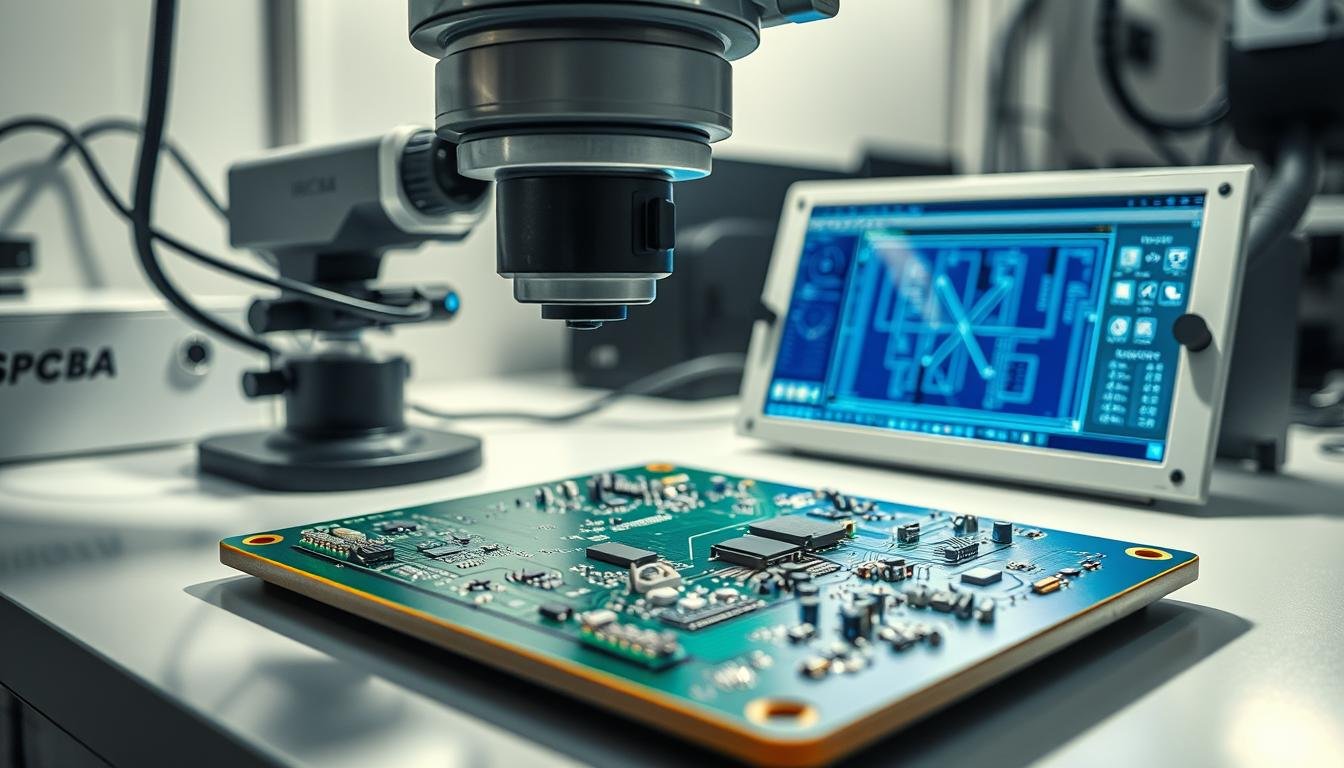
How 3D SPI Technology Works
 technology. In the foreground, a state-of-the-art 3D SPI machine with precision optics and advanced sensors, capturing intricate solder paste deposits on a printed circuit board. The middle ground showcases a magnified, cross-sectional view of the solder joints, highlighting their shape, volume, and consistency. In the background, a sleek, futuristic laboratory setting with clean lines and high-tech instrumentation, conveying the sophisticated nature of this quality control solution. Crisp lighting from multiple angles accentuates the depth and texture of the components, while a subtle blue-tinted color scheme evokes a sense of technical prowess and innovation.")
The advent of 3D SPI technology has revolutionized the solder paste inspection process in PCB manufacturing. This advancement has significantly improved the accuracy and efficiency of detecting defects in solder paste deposition.
Evolution from 2D to 3D SPI Systems
Traditional 2D SPI systems relied on cameras to capture flat images of solder paste deposits, which could detect basic issues like missing paste or misalignment. However, modern 3D SPI systems have taken this a step further by utilizing laser or structured light technology to create a three-dimensional view of the solder paste deposits. This allows for precise measurements of key parameters like solder paste volume, height, and area, providing a more accurate assessment of quality.
Key Components of Modern SPI Machines
Modern SPI machines are equipped with advanced components that enable high-precision inspection. These include:
- Illumination systems for optimal lighting
- High-resolution cameras for detailed imaging
- Optical systems for precise measurement
- Advanced image processing software for accurate analysis
These components work together to provide a comprehensive inspection of solder paste deposits, ensuring that even the smallest defects are detected.
The Inspection Process Step-by-Step
The SPI inspection process involves several critical steps:
- PCB loading: The PCB is loaded into the SPI machine.
- Image capture: The machine captures detailed images of the solder paste deposits.
- 3D reconstruction: The images are used to create a 3D model of the solder paste.
- Measurement and analysis: The machine measures key parameters and compares them against predetermined specifications.
- Defect detection and reporting: Any defects are identified and reported for further action.
This step-by-step process ensures that solder paste defects are caught early, preventing downstream issues in the PCB assembly process.
| Inspection Parameter | Measurement Capability |
|---|---|
| Solder Paste Volume | Precise measurement in cubic millimeters |
| Height | Measurement with micrometer precision |
| Area Coverage | Accurate assessment of paste spread |
By leveraging 3D SPI technology, manufacturers can significantly improve the quality of their PCB assemblies, reducing the risk of defects and enhancing overall production efficiency.
Critical Parameters Measured in Solder Paste Inspection
To guarantee the reliability of electronic components, SPI meticulously examines solder paste volume, height, area coverage, and alignment. These parameters are crucial in ensuring that the solder paste is applied correctly, directly impacting the quality of the final PCB assembly.
Solder Paste Volume and Its Significance
Solder paste volume refers to the total amount of paste deposited on each pad. Too little volume can lead to weak solder joints, while too much can cause bridging. 3D SPI systems measure solder paste volume in cubic micrometers to ensure it falls within a target range. This measurement is critical for preventing defects like insufficient connections or bridging.
Height and Area Coverage Measurements
The height of the solder paste deposit, typically measured in micrometers, is another vital parameter. Proper paste height (usually between 130-160 micrometers) ensures sufficient material for strong bonds while preventing excess that could lead to uneven soldering. Additionally, the area coverage indicates how much of the pad is covered by paste, with 90-100% coverage being ideal for optimal electrical and mechanical connections.
Alignment and Position Accuracy
Alignment refers to how accurately the solder paste is positioned on the pad. Even slight misalignments (beyond 25 micrometers) can cause components to shift during reflow soldering, potentially leading to defective solder joints. Thus, precise alignment is crucial for the overall quality of the PCB assembly.
Advanced Measurement Capabilities
Modern SPI systems offer advanced measurement capabilities, including surface roughness analysis, paste spread evaluation, and volumetric transfer efficiency calculations. These features enable comprehensive analysis and optimization of the solder paste application process.
| Parameter | Ideal Measurement | Significance |
|---|---|---|
| Solder Paste Volume | Within target range (cubic micrometers) | Prevents insufficient connections or bridging |
| Solder Paste Height | 130-160 micrometers | Ensures strong bonds without excess paste |
| Area Coverage | 90-100% | Optimal electrical and mechanical connections |
| Alignment | Within 25 micrometers | Prevents component shifting during reflow soldering |
Common Solder Paste Defects Detected by SPI

Solder Paste Inspection (SPI) is a critical process in Surface Mount Technology (SMT) assembly, enabling the detection of various defects that can compromise the quality of PCB assembly. The accuracy of SPI determines the reliability of solder joints, making it a vital step in ensuring high-quality PCB manufacturing.
Insufficient Solder Paste and Its Consequences
Insufficient solder paste on a pad can lead to weak or incomplete solder joints. This issue often arises due to stencil clogging or uneven pressure during the printing process. SPI detects insufficient solder paste by measuring low volume or reduced area coverage. For instance, if the solder paste volume is below 100 cubic micrometers or the area coverage is less than 80%, it flags the defect.
Excessive Solder Paste and Bridging Issues
Too much solder paste can cause solder bridging or tombstoning, where components lift off the board during reflow. SPI identifies excessive paste by flagging high volume or height values that exceed the acceptable range. For example, volumes above 150 cubic micrometers or heights over 180 micrometers are considered excessive. Bridging occurs when solder paste connects two adjacent pads, often due to overprinting or misalignment, potentially creating short circuits in the final product.
Misalignment Problems
Misalignment defects occur when solder paste deposits are offset from their intended positions. This can lead to component shifting and connection failures during the reflow process. SPI systems measure the alignment of solder paste deposits, detecting any deviations from the specified positions. By identifying misalignment issues early, manufacturers can prevent downstream defects and improve overall PCB quality.
Uneven Distribution and Other Defects
Uneven distribution of solder paste, along with other defects like solder balling, slumping, and print definition issues, can be detected through SPI. Modern SPI systems categorize and classify different types of defects using sophisticated algorithms, distinguishing between critical, major, and minor issues. By analyzing SPI data, manufacturers can identify patterns in defect occurrence, enabling targeted process improvements rather than simple pass/fail decisions.
Integrating SPI into the SMT Assembly Line
The strategic placement of SPI equipment in the SMT assembly line significantly enhances the overall quality of PCB manufacturing. By positioning SPI immediately after the solder paste printing stage and before component placement, manufacturers can detect and correct solder paste-related issues promptly.
Optimal Placement Within the Production Process
Optimal SPI placement is critical for maximizing its effectiveness. Typically, SPI is positioned after solder paste printing and before component placement. This allows for the immediate detection of solder paste defects, enabling corrective actions to be taken before proceeding with component placement.
Inline vs. Offline SPI Systems
Manufacturers can choose between inline and offline SPI systems based on their production needs. Inline SPI systems are integrated directly into the production line, enabling real-time, 100% inspection. Offline SPI systems, on the other hand, are separate from the main production line and offer more detailed inspection capabilities.
| SPI System Type | Integration | Inspection Capability |
|---|---|---|
| Inline SPI | Directly into production line | Real-time, 100% inspection |
| Offline SPI | Separate from main production line | More detailed inspection |
Creating Effective Feedback Loops
To maintain consistent quality, it’s essential to create effective feedback loops between SPI systems and solder paste printers. This enables automatic process adjustments, ensuring that solder paste application remains within specified parameters.
Best Practices for Maximizing SPI Effectiveness
To maximize the effectiveness of Solder Paste Inspection (SPI) in ensuring high-quality PCB assembly, manufacturers must adhere to best practices that enhance the accuracy and reliability of the inspection process. By implementing these practices, companies can significantly improve the quality of their SMT assembly lines and reduce costly defects.
Setting Appropriate Inspection Parameters
Setting the right inspection parameters is crucial for effective SPI. This involves defining acceptable ranges for solder paste volume, height, and alignment based on specific project requirements. Establishing meaningful thresholds that balance quality needs with production efficiency is key. For instance, manufacturers should consider factors like component type, PCB design, and the specific requirements of their SMT assembly process. By doing so, they can minimize false positives and negatives, ensuring that inspection results accurately reflect paste quality.
Regular Calibration and Maintenance
Regular calibration and maintenance of SPI equipment are essential to ensure measurement accuracy and extend the lifespan of the system. A deviation of just 10 micrometers can affect results, highlighting the importance of precise calibration. Manufacturers should follow a regular maintenance schedule, cleaning and calibrating their SPI systems as recommended by the manufacturer. This practice helps maintain the accuracy of measurements like solder paste height and volume, ensuring reliable inspection results.
Operator Training and Data Interpretation
Operator training is critical for maximizing the value of SPI investments. By equipping their teams with the skills to interpret SPI data and make quick adjustments to the printing process, manufacturers can significantly improve their SMT assembly lines. Effective training should cover how to use SPI data for process monitoring and continuous improvement, transforming inspection results into actionable insights for manufacturing optimization.
By following these best practices, manufacturers can optimize their SPI processes, leading to improved quality, reduced defects, and increased efficiency in their PCB assembly operations.
Conclusion: The Future of SPI in Electronics Manufacturing
As we look to the future of electronics manufacturing, SPI stands out as a crucial element in ensuring quality and reliability. The integration of artificial intelligence (AI) and machine learning into SPI systems is revolutionizing the industry by enabling predictive defect prevention. We are witnessing a significant shift towards Industry 4.0 principles, where SPI machines become connected nodes within smart factories, facilitating real-time process adjustments.
This transformation is crucial as PCB designs become increasingly complex and components continue to shrink. By leveraging advanced SPI technology, manufacturers can achieve unprecedented quality control and reduce defect rates to below 1%. We believe that investments in SPI technology today will position electronics manufacturers for success in the increasingly complex and quality-driven future of the industry.
By embracing these advancements, we can ensure that our manufacturing processes remain competitive and aligned with the evolving demands of the electronics manufacturing landscape.