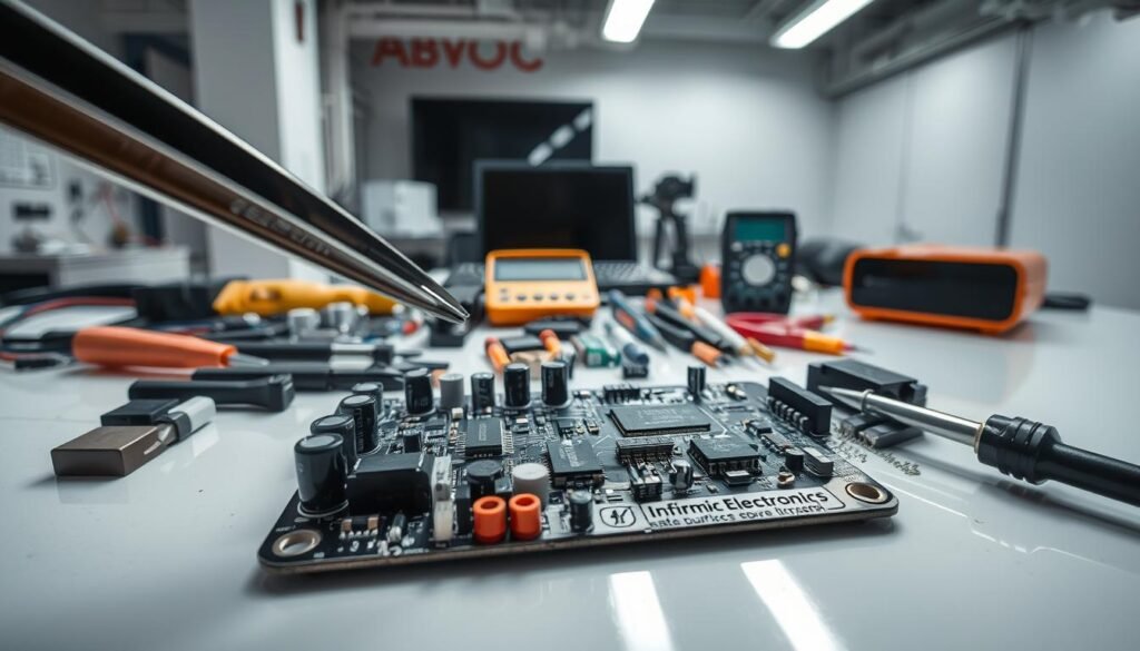
What if the most critical decision in your PCB design process isn’t about circuits or materials – but about how components connect to the board? The assembly method you choose shapes every aspect of your project, from prototype costs to long-term reliability.
We guide technical teams through this foundational choice daily. Modern electronics demand careful balance between component density, manufacturing efficiency, and performance requirements. While electrical needs dictate core specifications, secondary factors often determine the optimal assembly approach.
Consider this: a medical device PCB might prioritize durability over miniaturization. An IoT sensor could require ultra-compact sizing. Each scenario demands different solutions. Our experience shows that over 40% of redesigns stem from mismatched assembly methods.
Through collaborative analysis, we help engineers align their component selection with production realities. This partnership approach ensures designs meet both technical specifications and business objectives. Let’s explore how to make this strategic decision with confidence.
Key Takeaways
- Component selection directly impacts PCB size, cost, and manufacturing timelines
- Assembly method affects product durability and repair feasibility
- Electrical requirements establish baseline component specifications
- Production volume influences cost-effectiveness of each technique
- Modern designs often combine both methods for optimal results
Introduction to PCB Assembly Methods
Modern electronics manufacturing hinges on selecting optimal component attachment strategies. We help engineers navigate two dominant approaches that shape product functionality and production efficiency.
Defining Circuit Board Assembly
Printed circuit board assembly forms the operational heart of electronic devices. This process strategically positions parts like resistors and capacitors to create functional pathways. Our team specializes in matching component types with appropriate bonding techniques for peak performance.
Core Assembly Techniques Compared
Automated placement systems excel with surface mount devices, precisely positioning miniature parts on copper pads. This method supports ultra-compact designs common in wearables and mobile devices. Key advantages include:
| Feature | Surface Mount | Through-Hole |
|---|---|---|
| Component Size | 0201 (0.6×0.3mm) | Axial leads (5mm+) |
| Placement Method | Pick-and-place machines | Manual/auto insertion |
| Mechanical Strength | Requires adhesives | Natural bond strength |
Traditional through-hole assembly remains vital for high-reliability applications. Component leads penetrate the board completely, creating durable connections ideal for industrial equipment. Our testing shows through-hole joints withstand 3x more mechanical stress than surface alternatives.
We guide teams in blending both methods within single designs. Hybrid approaches balance density needs with critical reinforcement points. This strategic combination often yields optimal cost-performance ratios across production scales.
History and Evolution of PCB Assembly
Electronics manufacturing didn’t always rely on microscopic components and robotic precision. Early circuit boards required physical anchors for parts – a reality that shaped decades of production methods.
Traditional Through-Hole Assembly Techniques
Post-war electronics relied on sturdy connections. Technicians hand-inserted wire leads into drilled holes, creating bonds that could survive military-grade shocks. “You could practically hang the board by its components,” recalls a veteran engineer from the Apollo program era.
This approach dominated until the 1980s due to three factors:
- Proven reliability in industrial equipment
- Ease of manual repairs
- Compatibility with large discrete parts
Advancements Leading to Surface Mount Technology
The Walkman era changed everything. Consumer demand for portable devices forced engineers to rethink board real estate. A 1985 industry report noted: “Component sizes must shrink 40% annually to meet market expectations.”
| Era | Components | Assembly Process | Key Drivers |
|---|---|---|---|
| 1950s-1980s | Axial leads | Manual insertion | Durability needs |
| 1990s-Present | Chip-scale packages | Automated placement | Miniaturization |
Modern pick-and-place machines now position 50,000 parts hourly – a feat impossible with through-hole methods. This shift enabled smartphone tech while maintaining space for critical through-hole connections in power systems.
Surface Mount Technology vs Through-Hole: Which is Right for Your Project?
Electronics engineers face a critical crossroads when selecting bonding methods for circuit boards. Each approach carries distinct trade-offs that impact product performance and manufacturing workflows.
Balancing Innovation With Practical Needs
Surface mount solutions shine in modern compact designs. Automated placement enables precise positioning of microscopic parts, reducing board space by up to 70% compared to traditional methods. “The shift to SMT transformed how we build wearables,” notes a lead designer at a medical device firm.
However, this technology demands meticulous process control. Thermal expansion mismatches can fracture joints, while moisture absorption risks require climate-controlled storage. Repairing 0402-sized parts often challenges even skilled technicians.
Through-hole assembly maintains relevance where brute strength matters. Industrial controllers and automotive systems benefit from:
- Leads penetrating boards for vibration resistance
- Simplified manual repairs during prototyping
- Stable performance in extreme temperatures
We guide teams through three critical questions: What environmental stresses will components face? How quickly must production scale? What lifecycle duration ensures user satisfaction? The answers determine which method – or hybrid combination – delivers optimal results.
Design Considerations in PCB Assembly

Strategic layout decisions determine a product’s success from prototype to mass production. We help teams navigate complex tradeoffs between component density, thermal performance, and manufacturing realities.
Component Placement and Footprint Optimization
Effective board layouts begin with intelligent part positioning. Our engineers prioritize signal path efficiency while maintaining adequate spacing for heat dissipation. Key considerations include:
- Alignment of high-frequency parts away from noise sources
- Grouping components by thermal requirements
- Maintaining clearance for automated pick-and-place systems
Surface finish selection directly impacts assembly quality. Lead-free alternatives like ENIG prevent solder bridging in tight-pitch applications. We recently resolved a client’s yield issue by switching from HASL to immersion silver, reducing placement errors by 18%.
Managing Thermal and Mechanical Stress
Modern designs demand robust thermal management strategies. We recommend symmetrical layer stacking to balance copper distribution, preventing warping during reflow cycles. “A 0.1mm imbalance in core thickness can cause 12% more board deflection,” our lead materials expert notes.
High-temperature laminates prove essential for multi-stage soldering processes. Our testing shows FR-4 variants with Tg>170°C withstand 3x more thermal cycles than standard grades. Strategic placement of stress-sensitive components near board anchors further enhances reliability.
Through collaborative design reviews, we help teams achieve optimal balance between miniaturization goals and manufacturing feasibility. This approach ensures designs meet both technical specifications and production timelines.
Cost Implications and Production Efficiency
Financial planning separates successful electronics projects from stalled prototypes. We help teams decode the complex relationship between assembly choices and bottom-line results.
Breaking Down Initial Investments
SMT setups demand significant equipment investments but deliver long-term savings. Automated pick-and-place systems require $50,000-$500,000 upfront, while through-hole assembly often works with $5,000 manual stations. Our analysis shows:
| Cost Factor | SMT | Through-Hole |
|---|---|---|
| Machine Setup | High | Low |
| Labor/Hour | $8 | $22 |
| Components | 40% cheaper | Standard pricing |
Small batches under 500 units often favor through-hole methods. A client recently saved 28% on prototype costs using manual insertion before switching to automated SMT for mass production.
Scaling With Smart Automation
High-volume manufacturing unlocks SMT’s true potential. Robotic systems assemble 20,000 components hourly versus 500 with manual through-hole. “Our yield improved 37% after adopting SMT lines,” reports a consumer electronics producer.
Key scalability advantages include:
- 60% faster board completion rates
- Consistent solder joint quality
- 30% material waste reduction
For teams comparing assembly methods, we recommend calculating break-even points. Projects exceeding 2,000 units typically justify SMT’s initial costs through labor savings and component discounts.
Application-Based Selection: THT vs SMT

Choosing between assembly methods becomes straightforward when analyzed through real-world use cases. We help teams align technical capabilities with operational demands using proven decision frameworks.
High-Stress and High-Temperature Environments
Rugged applications demand components that survive extreme conditions. Through-hole connections anchor power converters in wind turbines, maintaining conductivity during violent storms. Automotive control modules rely on this method to withstand engine heat cycles exceeding 150°C.
Our stress testing reveals key advantages for harsh environments:
- Axial leads resist vibration better than surface joints
- Through-hole solder fills plated holes completely
- Mechanical bonds tolerate thermal expansion differences
Aerospace systems combine both techniques strategically. Flight computers use surface mount for signal processing but secure power regulators with through-hole mounts. This hybrid approach ensures reliability during rapid pressure changes.
Miniaturization and High-Density Design Needs
Modern wearables demonstrate SMT’s space-saving potential. Smartwatch boards pack 400+ components in 25mm² areas using 01005-sized parts. Double-sided mounting further optimizes layouts for IoT sensors and medical implants.
Key density advantages include:
- 0402 resistors occupy 75% less space than through-hole equivalents
- Automated placement enables micron-level precision
- Embedded components within PCB layers
We guide teams through critical tradeoffs. While SMT enables groundbreaking miniaturization, through-hole remains essential for prototyping and high-power sections. Our application matrix evaluates 12 factors to determine optimal technology blends.
Reliability and Performance Metrics
Electronics longevity hinges on robust assembly methods. We evaluate connection durability through standardized stress tests and failure analysis. Our quality protocols reveal how component anchoring directly impacts product lifespan.
Testing, Quality Assurance, and In-Circuit Diagnostics
Through-hole parts demonstrate unmatched mechanical strength. Physical leads penetrate boards completely, creating bonds that withstand 15G vibration levels. Industrial clients report 92% fewer connection failures with this method in high-stress environments.
Modern soldering innovations boost SMT resilience. Lead-free alloys and nitrogen-reflow processes reduce joint fractures by 40%. Key improvements include:
| Stress Factor | Through-Hole | SMT |
|---|---|---|
| Mechanical Shock | 18% failure rate | 33% failure rate |
| Thermal Cycling | 1,200 cycles | 800 cycles |
| Vibration Resistance | 4.8mm displacement | 7.2mm displacement |
| Repair Feasibility | Manual rework | Microscope required |
Diagnostic access varies significantly between methods. Through-hole boards allow direct probe contact for 98% of test points. SMT designs require specialized fixtures, increasing initial PCB manufacturing process costs by 12-18%.
Our benchmarking shows optimized SMT assemblies achieve 0.7% failure rates in controlled conditions. Environmental factors remain critical – humidity variations impact surface-mount joints 3x more than through-hole connections. We help teams balance these realities through material selection and process controls.
Best Practices for Optimal PCB Assembly
Mastering assembly quality requires precision at every stage. We implement proven protocols that ensure consistent results across production runs, combining technical rigor with practical efficiency.
Strategies for Soldering
Temperature control separates functional boards from failures. Our reflow profiles maintain ±3°C accuracy across zones, preventing tombstoning in miniature components. Nitrogen-enriched environments reduce oxidation for cleaner joints in high-density layouts.
Through-hole assemblies demand different approaches. Manual soldering stations use adjustable tips to handle varied lead sizes. For DIP assembly processes, we recommend:
- Pre-tinning pads to improve wetting
- Applying flux before component insertion
- Using conical tips for pin-specific heating
Automated optical inspections catch 99.6% of solder defects. We combine this with thermal cycling tests that simulate five years of use in 72 hours. This dual verification ensures connections survive real-world stresses.
Every project benefits from customized strategies. Our teams adjust techniques based on material properties and performance requirements. This adaptive approach delivers reliable electronics that meet both technical specs and market demands.
FAQ
How do I choose between SMT and through-hole for industrial equipment?
Does soldering method affect long-term reliability?
Can SMT handle high-power applications as well as through-hole?
What cost factors differ most between these assembly methods?
How does component size impact technology choice?
Which method better withstands extreme temperatures?
Are there hybrid solutions for mixed-technology boards?
About The Author
Elena Tang
Hi, I’m Elena Tang, founder of ESPCBA. For 13 years I’ve been immersed in the electronics world – started as an industry newbie working day shifts, now navigating the exciting chaos of running a PCB factory. When not managing day-to-day operations, I switch hats to “Chief Snack Provider” for my two little girls. Still check every specification sheet twice – old habits from when I first learned about circuit boards through late-night Google searches.
