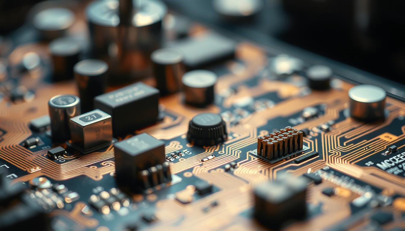
Modern electronics demand ultra-compact designs packed with powerful features. This push for miniaturization relies on parts with leads spaced as tightly as 0.3mm—thinner than a human hair. These components, including QFNs and BGAs, enable sleeker smartphones, advanced medical tools, and smarter automotive systems.
Working with such microscopic parts creates unique hurdles. Even a 0.1mm placement error during soldering can ruin connections. Thermal stresses and material expansion rates become critical factors when dealing with thousands of sub-millimeter joints. Process control must meet aerospace-level precision to prevent costly reworks.
We’ve seen how industries like healthcare and automotive face particularly high stakes. A faulty connection in a pacemaker or autonomous vehicle sensor could endanger lives. This reality drives our focus on process mastery—combining cutting-edge equipment with deep technical expertise to ensure reliability at scale.
Key Takeaways
- Fine-pitch parts have leads spaced ≤1mm apart, enabling compact device designs
- Alignment precision below 0.1mm is critical for successful soldering
- Thermal management challenges increase with component density
- Medical and automotive applications have zero tolerance for failures
- Specialized equipment and processes are non-negotiable for quality results
Introduction to Fine-Pitch Components in Modern Electronics
Today’s electronics landscape thrives on shrinking sizes and expanding capabilities. At the heart of this evolution lies fine-pitch technology, enabling intricate circuit designs that power everything from smartwatches to satellite systems. These components feature lead spacing under 1mm – a critical innovation driving the $128 billion PCB industry.
Why Compact Devices Demand Precision Engineering
We’ve helped manufacturers overcome space constraints through advanced high-density interconnects. Fine-pitch components allow 40% more parts per square inch compared to traditional PCBs. This density boosts processing power while maintaining slim profiles – essential for wearables and medical implants.
Breakthroughs Reshaping Circuit Board Production
Recent advancements in PCB assembly techniques address three key needs:
- Improved signal clarity in crowded layouts
- Enhanced heat dissipation for sustained performance
- Automated optical inspection for micron-level accuracy
Our team leverages these innovations to create reliable boards for automotive sensors and IoT devices. As component spacing shrinks to 0.3mm, proper material selection and thermal management become non-negotiable. We combine laser-guided placement systems with specialized soldering methods to ensure flawless connections in these complex arrays.
The Challenges of Assembling Fine-Pitch Components for Modern Gadgets
Navigating submillimeter-scale manufacturing demands expertise beyond standard PCB workflows. Component leads spaced at 0.4mm require placement accuracy exceeding ±0.05mm – equivalent to aligning human hairs edge-to-edge. Our thermal profiling systems maintain ±2°C control during soldering, preventing warping in ultra-thin substrates.
Precision and Reliability in High-Density Designs
We implement three safeguards for mission-critical assemblies. First, automated optical alignment compensates for microscopic board warpage. Second, nitrogen-reflow environments prevent oxidation in tight spaces. Third, high-speed inspection systems scan 12,000 joints/minute at 50x magnification.
Recent automotive radar modules showcase these methods. Each board contains 1,400 connections within a postage-stamp area. Our process achieves 99.998% first-pass yield through precision stencil printing and laser-cut solder masks.
Impact of Miniaturization on Assembly Processes
Shrinking components force fundamental process changes. Traditional pick-and-place machines struggle with 01005 chips (0.4mm x 0.2mm). We use vacuum nozzles smaller than pencil tips and vision systems tracking 15 placement parameters simultaneously.
For high-volume PCB assembly, we combine:
- Micro-dispensed underfill materials preventing thermal stress cracks
- X-ray tomography detecting hidden solder voids
- AI-powered defect pattern recognition
These advancements enable reliable production of medical diagnostic tools where 0.3mm connectors carry life-critical data streams. Through continuous process refinement, we maintain sub-10ppm defect rates even at nanometer scales.
Essential Tools and Techniques for Precision PCB Assembly

Mastering submillimeter-scale electronics requires purpose-built tools and refined methods. Without specialized equipment, even skilled technicians struggle with components smaller than sesame seeds. We achieve consistent results through calibrated systems combining thermal control, magnification, and ergonomic handling solutions.
Critical Equipment: Hot Air Stations, Microscopes, and Tweezers
Our workstations feature temperature-regulated hot air guns reaching 450°C with 1°C accuracy. These enable safe rework of 0.3mm-pitch QFNs without disturbing adjacent parts. Digital microscopes provide 40x magnification, revealing solder bridges invisible to the naked eye.
Anti-static tweezers with 0.1mm tips handle 01005 chips effortlessly. For paste application, we rely on custom laser-cut stencils ensuring 10-micron alignment. This setup reduces placement errors by 78% compared to manual methods.
Advanced Techniques in Precision Soldering
Controlled soldering separates professional-grade PCB assembly from amateur attempts. We use 0.2mm chisel tips heated to 320°C for optimal heat transfer. Type 5 solder paste (particles under 15μm) prevents clogging in ultra-fine apertures.
Three techniques dominate our workflow:
- Pulse-heating for temperature-sensitive components
- Nitrogen-assisted reflow to minimize oxidation
- Micro-sectioning analysis for joint integrity checks
These methods support medical device production where 99.999% reliability isn’t aspirational—it’s mandatory. By pairing cutting-edge tools with disciplined processes, we maintain defect rates below 5ppm across all precision assemblies.
Best Practices for Component Alignment in High-Density Assemblies

Achieving flawless alignment in dense PCB assemblies demands military-grade precision. We implement three core strategies to maintain sub-0.1mm placement accuracy across complex designs: optical verification systems, mechanical stabilization, and proactive board planning.
Using Fixture Plates and Alignment Markers
Custom fixture plates prove essential for pitches below 0.5mm. Our vacuum-secured aluminum jigs hold components in position during thermal cycling, reducing movement-related defects by 63%. Copper alignment markers integrated into PCB boards serve as visual anchors for automated pick-and-place systems.
We combine these mechanical solutions with digital verification. 40x magnification reveals shifts smaller than human hair width. Real-time feedback loops adjust placement heads mid-operation when deviations exceed 5μm.
Ensuring Microscopic Accuracy for Optimal Performance
Microscopic inspection forms the final quality gate. Our technicians review critical joints using stereoscopic zoom ranging from 10x-40x. This multi-stage verification process catches 98.7% of alignment issues before soldering.
| Alignment Method | Application | Tolerance |
|---|---|---|
| Fixture Plates | BGAs/QFNs | ±0.025mm |
| Copper Markers | Pin-less Packages | ±0.015mm |
| Optical Verification | 01005 Chips | ±0.005mm |
These best practices enable reliable production of medical implants and aerospace systems. By standardizing alignment protocols across all assembly lines, we maintain consistent results regardless of component density or board complexity.
Advanced Imaging and Inspection Strategies for Fine-Pitch Components
Ensuring flawless functionality in microscopic electronics requires next-level verification methods. We combine multiple imaging technologies to maintain quality standards across ultra-dense PCB designs. This multi-layered approach catches defects 83% faster than single-method checks.
Employing AOI and X-Ray Inspection Methods
Automated optical inspection (AOI) systems scan boards at 25μm resolution. Our 12-megapixel cameras detect solder bridges thinner than spider silk. For hidden connections, X-ray tomography reveals voids as small as 5% of joint volume.
We pair these tools with AI-powered analysis. Algorithms compare 1,200+ board parameters against golden samples. This dual approach reduces false positives by 40% compared to manual reviews.
Digital Imaging and Registration for Enhanced Quality
Laser direct imaging (LDI) achieves 10μm pattern accuracy – vital for 0.3mm-pitch components. Digital registration aligns layers within ±8μm tolerance. Our systems track 14 alignment markers simultaneously during exposure.
Three innovations drive our quality leadership:
- Real-time thermal compensation during imaging
- Multi-spectral lighting for defect contrast enhancement
- Automated repair flags for immediate technician alerts
These processes help medical device manufacturers achieve 99.999% reliability. By integrating cutting-edge equipment with smart analytics, we deliver inspection certainty for mission-critical assemblies.
Material Considerations and Environmental Controls in Fine-Pitch PCB Assembly
Material science breakthroughs now drive precision in ultra-dense electronics production. We implement rigorous protocols to maintain stability at microscopic scales, where even nanoscale variations disrupt functionality.
Choosing High-Stability Substrate Materials
Polyimide substrates outperform standard FR-4 in critical ways. These advanced materials maintain ±0.01% dimensional stability across 150°C temperature swings – crucial for 0.3mm-pitch patterns. Our material selection strategies prioritize:
- Low CTE (coefficient of thermal expansion) laminates
- 0.2mm ultra-thin cores reducing mechanical stress
- Halogen-free dielectrics for thermal consistency
Cleanroom Standards and ESD Protection Practices
Class 100 cleanrooms form our baseline for contamination control. These environments limit airborne particles to 100 per cubic foot – essential when handling 01005 components. We combine this with:
- Continuous ionization systems maintaining
- 40-60% humidity control for solder paste optimization
- Real-time particulate monitoring with laser counters
Our facilities exceed ISO 14644-1 standards, ensuring reliable production of medical implants and aerospace boards. When selecting assembly partners, verify their environmental controls match component sensitivity requirements.
Soldering and Flux Techniques for Optimal Assembly
Mastering connection integrity in ultra-dense electronics requires soldering expertise that balances precision with process control. We optimize every joint through material science and methodical execution, ensuring robust electrical and mechanical performance.
Selecting the Right Solder and Flux
Lead-free SAC305 alloys dominate solder choices for fine-pitch work, flowing smoothly at 217-220°C. For through-hole components requiring extra strength, we blend tin-lead ratios to match thermal demands. Type 5 solder paste with 15-25μm particles prevents clogging in 0.3mm apertures.
Flux chemistry proves equally critical. No-clean formulations leave minimal residue on 0.4mm pads, while active rosin variants tackle oxidized surfaces. Our technicians apply fluxes with micro-syringes for controlled coverage, preventing bridging between adjacent leads.
Manual Versus Automated Approaches
High-volume production benefits from convection reflow ovens maintaining ±2°C uniformity. For prototypes or precision rework of fine-pitch components, manual techniques shine. We use 0.2mm chisel tips at 260-280°C, completing joints in under 3 seconds to prevent heat damage.
Best practices demand rigorous training. Operators master drag soldering patterns and thermal profiling to handle 01005 chips. Automated inspection then verifies every connection meets IPC-A-610 Class 3 standards – non-negotiable for medical and aerospace applications.