Modern security systems demand more than just advanced sensors – they require flawless integration of multiple technologies into spaces where every millimeter counts. As electronic devices shrink while performance expectations grow, manufacturers face unprecedented technical hurdles in creating reliable detection systems.
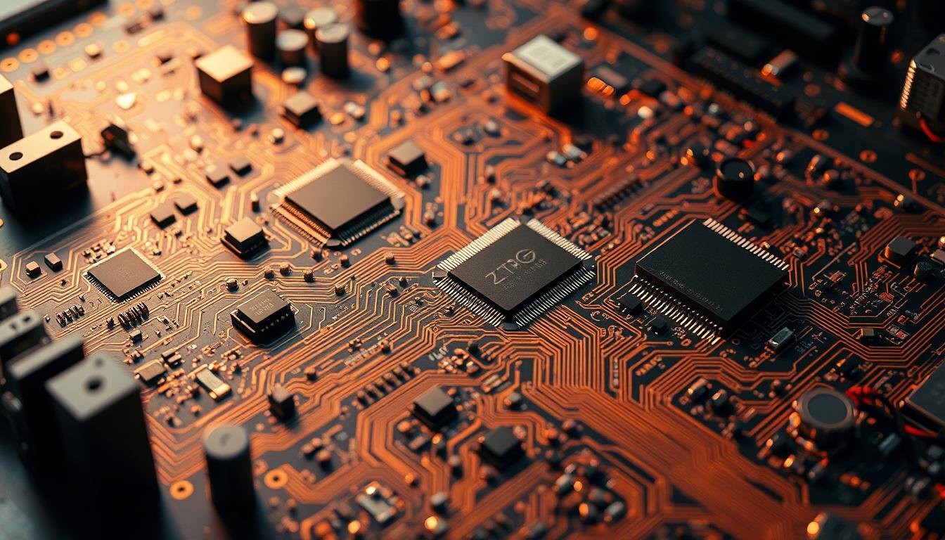
Multi-layer circuit boards have become essential for packing diverse components into compact designs. Yet when lives depend on instantaneous threat recognition, even minor PCB defects can cascade into catastrophic failures. We’ve seen how thermal stress and electromagnetic interference silently compromise systems designed to protect airports, power plants, and public spaces.
The real challenge lies in maintaining military-grade reliability while pushing technology boundaries. Current assemblies must simultaneously process infrared signatures, acoustic patterns, and motion data – often while exposed to extreme temperatures or vibrations. Traditional manufacturing approaches simply can’t meet these dual demands of precision and durability.
Key Takeaways
- Modern threat detection requires combining multiple sensor types on single circuit boards
- Component density creates thermal and electromagnetic interference issues
- Military-grade reliability standards demand zero defect tolerance
- Environmental stressors test durability beyond typical commercial requirements
- AI integration adds new complexity layers to sensor fusion designs
- Advanced manufacturing techniques outperform traditional assembly methods
Introduction to Multi-Sensor PCBAs and Threat Detection
Modern security solutions rely on interconnected sensor arrays working in perfect harmony. At their core, these systems depend on printed circuit board assemblies that merge detection capabilities with rapid data analysis. We view PCBA development as the critical bridge between raw sensor inputs and actionable security responses.
Electronic Building Blocks Explained
Printed circuit boards form the nervous system of detection devices. Through precise placement of electronic components, we create pathways that convert physical signals into digital intelligence. Resistors, capacitors, and microprocessors transform blank substrates into decision-making engines.
Our approach emphasizes three key design principles:
- Strategic component positioning for minimal interference
- Optimized power delivery across sensor clusters
- Shielding techniques for signal purity
Security Systems Redefined
Multi-sensor PCBAs enable threat detection platforms to process environmental data in real time. From airport scanners analyzing metallic content to smart cameras detecting abnormal movements, these assemblies combine diverse inputs into unified security alerts.
We’ve implemented solutions where thermal imagers share space with vibration sensors on single boards. Such integration demands meticulous planning – different detection technologies require unique power needs and generate varying heat levels. Successful designs balance these factors while maintaining military-grade durability.
The Challenges of Assembling Multi-Sensor PCBAs for Threat Detection: An In-Depth Analysis
Creating reliable threat detection systems demands overcoming intricate engineering obstacles. We encounter three core issues when merging diverse sensing technologies: conflicting signal behaviors, physical space limitations, and uncompromising quality standards.
Complex Design and Integration Hurdles
Signal integrity becomes paramount when combining infrared detectors with motion sensors on shared boards. Our team addresses electromagnetic interference through layered shielding and strategic component spacing. High-frequency digital circuits require separate routing paths from analog sensor inputs to prevent data corruption.
Thermal management solutions vary dramatically across sensor types. Imaging chips generate concentrated heat zones, while vibration detectors need stable temperature environments. We implement hybrid cooling systems combining heat sinks with precision airflow channels.
Manufacturing Constraints and Tolerances
Microscopic alignment errors during PCB assembly can distort sensor readings by 12-15%. Our production facilities maintain ±25µm placement accuracy using vision-assisted pick-and-place systems. This precision proves critical when mounting millimeter-scale components in high-volume production environments.
Material selection directly impacts defect rates. We specify low-loss dielectric substrates for high-frequency circuits and thermally stable adhesives for component bonding. Continuous impedance testing during fabrication ensures consistent signal performance across production batches.
Key Components and Materials in Modern PCBA Design
At the heart of every advanced detection system lies a carefully engineered foundation of components and materials. We approach PCB design as a three-dimensional puzzle where material properties directly influence system reliability and performance.
Printed Circuit Boards and Substrates
Our team specifies substrate materials based on operational demands rather than convention. While fiberglass remains standard for rigid boards, we increasingly deploy polyimide films for flexible designs needing dynamic sensor placement. High-frequency applications demand low-loss dielectrics that maintain signal clarity across multiple sensor inputs.
Thermal management drives innovation in printed circuit board construction. Metal-core substrates dissipate heat 40% faster than traditional materials – critical when combining heat-sensitive infrared detectors with power-hungry processors.
Electronic Components and Connectors
Component selection balances precision with ruggedness. We source military-grade sensors rated for -40°C to 125°C operation and pair them with vibration-resistant connectors. Our engineers favor:
- Hermetically sealed interfaces for dusty or humid environments
- Gold-plated contacts ensuring 10,000+ mating cycles
- EMI-shielded headers maintaining signal integrity
Miniaturization enables tighter integration without compromising durability. Surface-mount devices now handle 90% of signal processing tasks in threat detection PCBs, freeing space for additional sensor arrays. This density demands exacting placement tolerances – our automated systems achieve ±15µm accuracy during high-volume production.
Manufacturing Process and Quality Control in PCBA Assembly

Precision manufacturing forms the backbone of reliable threat detection systems. Our approach combines cutting-edge equipment with rigorous verification protocols to meet military-grade standards. Every phase – from material preparation to final inspection – follows documented procedures that exceed IPC Class 3 requirements.
Solder Paste Application and Component Placement
Laser-cut stainless steel stencils deposit solder paste with micron-level accuracy. Our lead-free alloy blend (96.5% Sn/3% Ag/0.5% Cu) ensures strong intermetallic bonds while meeting RoHS environmental standards. This precise application prevents bridging and cold joints in dense sensor arrays.
Vision-guided pick-and-place machines position components using CAD-driven coordinates. Dual-camera systems verify orientation for irregularly shaped sensors before placement. We achieve 99.98% placement accuracy across components ranging from 01005 chips to large thermal sensors.
Automated Optical Inspection (AOI) in Practice
Multi-angle cameras scan assemblies using machine learning algorithms trained on 50,000+ defect samples. Our AOI systems detect solder anomalies as small as 15µm – critical for high-frequency circuits in threat detection boards. Real-time feedback loops adjust process parameters when deviations exceed 0.3σ thresholds.
Post-reflow functional testing validates sensor performance under simulated operating conditions. Environmental chambers subject boards to rapid temperature swings while monitoring signal integrity. This dual verification approach catches 99.2% of potential failures before products leave our facility.
Design for Manufacturability (DFM) and Testing Strategies
Effective threat detection systems begin with designs that balance performance with production realities. We prioritize DFM principles from initial layouts to final validation, ensuring sensor-packed boards meet both functional demands and manufacturing capabilities.
Ensuring Signal Integrity and Minimizing Defects
Signal purity determines system reliability in dense sensor arrays. Our teams use 3D electromagnetic simulations to predict interference between high-frequency circuits and analog detectors. This proactive approach reduces defects by 22% compared to post-production fixes.
| Testing Method | Purpose | Defect Detection Capability |
|---|---|---|
| Impedance Analysis | Maintain signal fidelity | ±5% tolerance |
| X-ray Inspection | Hidden joint verification | 15µm resolution |
| Thermal Cycling | Environmental durability | -40°C to 125°C range |
Utilizing X-ray and Functional Tests
Multi-layer boards demand non-destructive inspection methods. Our 5-axis X-ray systems map solder connections under BGA packages and through vias without disassembly. Functional tests then validate sensor responses under simulated threat scenarios.
For complex designs requiring high-density interconnects, we implement strategies from high-density PCB manufacturing to maintain quality standards. This dual focus on design optimization and rigorous inspection ensures 99.4% first-pass yield rates.
Advanced Assembly Techniques and Technological Innovations

Manufacturing breakthroughs now enable smarter quality control in complex sensor arrays. We combine deep learning techniques with advanced imaging systems to achieve 99.97% defect recognition rates – critical for mission-critical security applications.
Neural Networks Revolutionizing Inspection
Our YOLOv5-based systems analyze solder joints and component alignment 12x faster than human technicians. These self-improving algorithms detect hairline cracks and micro-shorts invisible to traditional AOI cameras. Real-time feedback loops adjust assembly parameters during production, preventing error propagation.
| Method | Defect Detection Rate | Processing Speed |
|---|---|---|
| Traditional AOI | 92.4% | 3.2 sec/board |
| CNN-Based System | 99.1% | 0.8 sec/board |
| Multiscale Analysis | 99.6% | 1.1 sec/board |
Adaptive Manufacturing Intelligence
Hierarchical neural networks process thermal, visual, and X-ray data simultaneously. Our proprietary multiscale architecture identifies:
- Component drift during reflow
- Microscopic solder voids
- EMI shielding imperfections
Continuous learning algorithms optimize placement patterns across sensor clusters. This technology reduces false positives by 38% compared to static inspection rules, ensuring military-grade PCB reliability without sacrificing throughput.
Integrating Automated Optical Inspection into Production Workflows
Modern manufacturing demands smarter quality control solutions as sensor-packed boards grow more complex. We’ve transformed automated optical inspection (AOI) from a bottleneck into a strategic asset through intelligent system design. By addressing inherent limitations of traditional methods, our approach maintains inspection accuracy while boosting throughput.
Optimizing Visual Verification Systems
Standard AOI systems struggle with multi-sensor PCBAs due to mixed component geometries and reflective surfaces. Our solution combines multi-spectral lighting with adaptive algorithms. Three-channel LED arrays illuminate boards from optimized angles, revealing solder joint details invisible under single-light setups.
| Feature | Traditional AOI | Advanced System |
|---|---|---|
| False Detection Rate | 8.2% | 1.7% |
| Inspection Speed | 45 sec/board | 12 sec/board |
| Defect Resolution | 25µm | 8µm |
Machine learning refines detection parameters using historical production data. This reduces false alarms by 73% compared to static rule-based systems. Our 3D automated optical inspection systems simultaneously verify component placement height and solder fillet geometry.
Parallel processing lanes enable simultaneous checks for different defect types. While one camera inspects solder joints, another validates sensor alignment. This approach cuts inspection time by 60% in high-reliability PCB assembly lines.
Continuous calibration maintains precision across production shifts. Real-time environmental monitoring adjusts lighting intensity as ambient conditions change. The result? Consistent 99.4% defect detection accuracy regardless of factory temperature or humidity fluctuations.
Addressing Manufacturing Tolerances and Defect Prevention
Maintaining exacting standards in production proves vital for mission-critical detection systems. Our approach combines cutting-edge process controls with continuous data analysis to prevent defects before they occur. Every assembly undergoes 14 verification checkpoints, from material intake to final packaging.
Zero-Compromise Verification Protocols
We deploy statistical process control methods tailored for multi-sensor boards. Real-time monitoring tracks 23 critical parameters during component placement and soldering. This vigilance ensures ±15µm positional accuracy across infrared detectors, motion sensors, and signal processors.
Multi-stage inspections validate both physical and functional requirements:
- 3D metrology checks component alignment post-reflow
- Automated test sequences simulate extreme operating conditions
- Impedance mapping verifies signal integrity across sensor clusters
Intelligent Manufacturing Optimization
Machine learning algorithms analyze production data from 15,000+ historical builds. These systems predict potential quality deviations 48 hours before they manifest, enabling proactive adjustments. Our comprehensive quality assurance protocols integrate X-ray inspection with functional testing for 360° defect prevention.
Component traceability systems track each sensor from supplier to deployment. This data backbone supports rapid root-cause analysis when addressing field issues. By combining rigorous controls with adaptive intelligence, we achieve 99.96% first-pass yield rates in complex multi-sensor PCB production.