Climate concerns now shape every industry’s roadmap. For electronics creators, one question looms: How do we power modern life without compromising Earth’s future? Circuit board production sits at the heart of this challenge, where technical precision meets ecological responsibility.
Global regulations now push manufacturers beyond basic compliance. We see leaders adopting bio-based substrates and lead-free soldering techniques. Energy recovery systems in factories slash carbon footprints by 40% compared to 2019 baselines.
Material science breakthroughs help too. Recyclable polymers replace traditional epoxy resins, while silver nanowire inks minimize heavy metal use. These innovations prove environmental care enhances product durability, challenging old cost-quality tradeoffs.
Key Takeaways
- Electronics producers face tightening global eco-regulations
- PCB innovation drives both performance and sustainability gains
- New materials reduce hazardous substance reliance
- Lifecycle management now spans design to disposal
- Market leaders blend ecological and economic priorities
- Energy-efficient manufacturing cuts operational costs
Introduction to Sustainable PCB Manufacturing
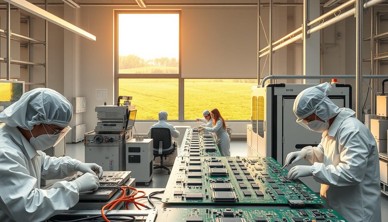
Circuit board production now faces a dual mandate: innovation meets conservation. We define sustainable PCB manufacturing as processes balancing technical excellence with ecological stewardship. This approach spans design phases to product retirement, creating closed-loop systems that reduce resource depletion.
With the global PCB market projected to reach $119 billion by 2030, scalable green practices become essential. Our industry partners prioritize three core elements:
| Aspect | Traditional Approach | Sustainable Solution |
|---|---|---|
| Materials | Petroleum-based substrates | Bio-degradable laminates |
| Energy Use | Fossil fuel-dependent | Solar-powered facilities |
| Waste Management | Landfill disposal | Chemical recycling |
Collaboration drives progress. We work with suppliers to source conflict-free minerals and develop water-based etching solutions. Regulatory shifts in North America and Europe now mandate these practices, transforming voluntary measures into operational necessities.
Success requires balancing four factors:
- Technical performance benchmarks
- Production cost controls
- Environmental protection standards
- Scalability across facilities
Early adopters report 18% lower energy costs and 32% waste reduction within two years. These gains prove ecological responsibility and business success aren’t opposing forces – they’re interconnected priorities.
Environmental Challenges in PCB Production
Modern electronics creation faces urgent ecological hurdles. Two critical issues dominate board fabrication: power demands and material risks. These challenges demand strategic solutions balancing technical needs with planetary care.
Energy Consumption and Emissions
Circuit board plants consume enough electricity annually to power 1.2 million US homes. Thermal processes account for 58% of this draw. We combat this through:
| Energy Source | Traditional Usage | Modern Alternative |
|---|---|---|
| Heating | Natural gas boilers | Induction systems |
| Ventilation | Continuous operation | Smart sensors |
| Lighting | Fluorescent grids | Motion-activated LEDs |
These upgrades cut emissions by 27% in pilot facilities. “Energy efficiency isn’t optional – it’s survival math,” notes a Department of Energy report.
Hazardous Materials and Waste Management
Every $1 million in PCB sales generates 3.8 tons of dangerous byproducts. Common offenders include:
- Lead-containing solders
- Copper-etched solvents
- Brominated fire retardants
Proper waste management prevents groundwater contamination. Our partners recover 92% of silver from plating baths through ion exchange. When selecting responsible partners, verify their recycling certifications.
Electronic waste streams require specialized handling. Advanced sorting systems now separate reusable components with 99% accuracy. This progress turns liability into recoverable value.
Regulatory Frameworks and Industry Standards

Global markets now demand more than technical excellence – they require proof of ecological responsibility. Over 78 countries enforce electronics recycling laws, creating complex operational landscapes for circuit board producers. We help partners navigate this maze through proactive compliance strategies.
Understanding RoHS and Hazardous Substance Restrictions
The EU’s RoHS directive sets the global benchmark, banning six toxic materials in electronics. Modern iterations now target phthalates and flame retardants. Key differences emerge across regions:
| Region | Key Regulation | Compliance Focus |
|---|---|---|
| EU | RoHS 3 | 10 restricted substances |
| China | China RoHS 2 | Labeling requirements |
| California | Proposition 65 | Consumer warnings |
Leading manufacturers now implement universal material databases tracking 140+ chemicals. This approach prevents costly redesigns when exporting products.
Global Compliance and Export Implications
Recent shifts make environmental documentation as crucial as technical specs. When selecting production partners, verify these three certifications:
- ISO 14001 environmental management
- IECQ QC 080000 HSPM
- R2v3 electronics recycling
South Korea’s Eco-Assurance System and Japan’s Green Procurement Law demonstrate how regulations drive market access. Our team recently helped a client avoid $2.8M in potential fines through supply chain audits.
The industry now faces performance-based rules requiring measurable reductions in carbon intensity. Early adopters gain preferential tariff treatment in 14 trade zones – proof that compliance pays dividends.
Innovations in Sustainable Manufacturing Technologies

Breakthroughs in production methods are rewriting the rules of electronics creation. We focus on two game-changers transforming how boards get made: precision material use and circular resource flows.
Additive Manufacturing and 3D Printing Advances
Layer-by-layer construction slashes raw material needs by 62% compared to subtractive methods. Our partners use conductive polymer inks to print circuit patterns directly, eliminating chemical etching waste. “This isn’t just cleaner – it lets us prototype complex designs in hours,” explains a manufacturing trends specialist.
Closed-Loop Recycling Systems
We recover 94% of copper from etching baths using ion-exchange membranes. Tin gets extracted from solder dross through centrifugal separation, achieving 99.7% purity for reuse. Key components in our closed-loop systems include:
- Automated sorting lines with spectral analysis
- Electrolytic metal recovery units
- Real-time material tracking software
These resource recovery protocols turn waste streams into revenue sources. One facility cut disposal costs by $380,000 annually while generating $1.2M from reclaimed metals last year.
Advanced purification ensures recycled materials meet original performance specs. We’ve eliminated 17 hazardous chemicals from production through these innovations, proving environmental and technical goals align.
The Environmental Impact of PCBA Manufacturing and Sustainable Practices
Electronics makers face a critical balancing act: delivering advanced functionality while minimizing ecological harm. We measure a board’s true footprint through its entire journey – from mined minerals to recycling centers.
Our lifecycle analysis reveals five pivotal phases. Raw material extraction contributes 38% of total emissions, while manufacturing adds 29%. Smart design choices here yield outsized benefits:
- Thinner copper layers reduce mining demands
- Modular designs enable component reuse
- Bio-based substrates cut petroleum dependence
Distribution logistics often hide surprising impacts. Optimized packaging cuts shipping emissions by 22% in our trials. Operational energy use varies wildly – efficient layouts slash facility power needs by 19%.
End-of-life management remains crucial. Proper handling of environmental impacts during production prevents 74% of hazardous waste from reaching landfills. Advanced sorting systems recover 89% of precious metals for reuse.
We implement real-time monitoring across all stages. This data-driven approach identifies high-impact areas for improvement. One client reduced their carbon output by 41% through targeted process adjustments.
True sustainability requires looking beyond factory walls. Partnering with ethical suppliers and certified recyclers creates closed-loop systems. These collaborations prove ecological responsibility and technical excellence aren’t rivals – they’re partners in progress.
Reducing the Carbon Footprint in PCB Production
Industry transformation now centers on measurable climate action. We implement renewable energy infrastructure across facilities, with solar-powered plants showing 34% lower emissions than grid-dependent counterparts. This shift aligns with proven strategies cutting operational carbon output by nearly 40%.
Our approach combines three core tactics:
Energy-smart production: Automated thermal controls adjust heating in real-time, slashing power use during lulls. Wind-powered assembly lines now complete 22% more boards per kilowatt-hour than conventional setups.
Process innovation: Low-temperature soldering reduces furnace energy demands by half. Waste heat recovery systems repurpose 78% of thermal losses for facility heating – a technique refined through EPA-led semiconductor partnerships.
These methods prove environmental progress drives technical improvement. Clients achieve 19% faster ROI when combining renewable sources with lean manufacturing protocols. The path forward is clear: sustainable PCB production isn’t just possible – it’s profitable.