Can a simple factor like PCB thickness significantly influence the overall performance and cost of your electronic device? The answer lies in understanding how this critical parameter affects the mechanical strength, thermal management, and manufacturing process of your printed circuit board assemblies.
We recognize that selecting the optimal PCB thickness is a complex decision that involves balancing performance requirements with budget constraints. As industry experts, we will explore how different board thicknesses impact various aspects of PCBA performance and manufacturing costs.
Our comprehensive guide will examine the trade-offs between thinner and thicker boards, providing data-driven insights to help you make informed decisions about PCB thickness that align with your specific application needs and cost parameters.
Key Takeaways
- Understanding how PCB thickness affects mechanical durability and electrical performance.
- Analyzing the impact of board thickness on thermal management and manufacturing complexity.
- Balancing performance requirements with budget constraints for optimal PCB thickness.
- Data-driven insights for informed decisions on PCB thickness.
- Trade-offs between thinner and thicker boards in PCBA manufacturing.
Understanding PCB Thickness Fundamentals
Understanding the basics of PCB thickness is essential for designing and manufacturing reliable electronic circuits. The thickness of a PCB is a critical parameter that affects not only the mechanical strength and durability of the board but also its electrical performance and manufacturability.
What Defines PCB Thickness
The thickness of a PCB is defined by the cumulative thickness of its substrate material, copper layers, solder mask, and other components. The substrate material, typically made from FR4 or other dielectric materials, forms the base thickness. Copper layers, which are used for signal and power distribution, add to the overall thickness. The industry has adopted standard PCB thickness measurements to ensure compatibility and reduce manufacturing costs.
Standard PCB Thickness Measurements
Standard PCB thickness measurements have been established to serve as benchmarks for different applications and manufacturing processes. Common PCB thickness selections include 0.8mm for space-constrained consumer electronics, 1.6mm as the universal standard for most applications, and 2.4mm to 3.2mm for applications requiring enhanced durability. These standard PCB thicknesses ensure compatibility with component lead lengths and manufacturing equipment, maintaining consistency in the supply chain.
We commonly work with various PCB thickness options, and the choice of thickness depends on the specific requirements of the project, including mechanical strength, weight, and electrical performance. By understanding and utilizing standard PCB thickness measurements, manufacturers can optimize their processes and reduce costs.
Factors That Determine PCB Thickness
Understanding the factors that determine PCB thickness is essential for optimizing both performance and cost in electronic designs. The thickness of a PCB is influenced by several critical elements, each contributing to its overall functionality and manufacturing complexity.
Substrate Material and Thickness
The substrate material is the foundation of a PCB, providing mechanical support and insulation between conductive layers. The choice of substrate material significantly affects the PCB’s thickness. Common materials include FR4, a glass-reinforced epoxy laminate known for its durability and cost-effectiveness. The thickness of the substrate can vary, typically ranging from 0.2 mm to several millimeters, depending on the application requirements.
Copper Layer Weight and Thickness
Copper layers are essential for the functionality of a PCB, enabling the transmission of electrical signals. The weight and thickness of these copper layers contribute to the overall PCB thickness. Standard copper thicknesses range from 0.5 oz to 3 oz or more per square foot, with thicker copper layers used for high-current applications. The copper thickness affects not only the PCB’s thickness but also its electrical performance and thermal management capabilities.
Prepreg Layers in Multilayer PCBs
In multilayer PCBs, prepreg layers are used to bond different layers together. Prepreg, short for “pre-impregnated,” is a material made by impregnating a glass fabric with a resin that is then partially cured. The number and thickness of prepreg layers can significantly impact the overall PCB thickness. The type of prepreg used, such as FR4 or high-speed materials, also influences the PCB’s electrical and thermal properties.
Solder Mask and Silkscreen Contribution
The solder mask and silkscreen layers, while thin, contribute to the overall PCB thickness. The solder mask, applied to protect copper traces from oxidation and solder bridging, typically adds 0.02 mm to 0.05 mm to the PCB thickness. The silkscreen layer, used for component designators and polarity markings, adds minimal thickness but is crucial for assembly. Modern manufacturing processes allow for precise control over the application of these layers, ensuring consistent quality.
| Layer | Typical Thickness Range | Contribution to PCB Thickness |
|---|---|---|
| Substrate | 0.2 mm – several mm | Significant |
| Copper Layers | 0.5 oz – 3 oz | Moderate to Significant |
| Prepreg Layers | Varies | Moderate |
| Solder Mask | 0.02 mm – 0.05 mm | Minor |
| Silkscreen | Minimal | Negligible |
The Impact of Board Thickness on PCBA Performance and Cost
In PCBA manufacturing, the thickness of the board is a key determinant of both cost and performance. The thickness of a PCB plays a crucial role in the manufacturing process, and designers must carefully consider the implications of their chosen thickness on the manufacturability of the board.
Direct Correlation Between Thickness and Manufacturing Expenses
Choosing a non-standard PCB thickness may lead to increased production costs and lead times. We advise clients that thicker boards often require specialized connectors and mounting hardware, which can increase bill of materials costs by 15-30% compared to standard thickness designs. Consulting with your PCB manufacturer during the design phase can help optimize production efficiency.
The manufacturing expenses are directly correlated with the thickness of the PCB. Thicker PCBs require more material and more complex manufacturing processes, which can drive up costs.
How Thickness Affects Overall Project Budget
Beyond direct manufacturing costs, PCB thickness significantly impacts the overall project budget through its influence on component selection, assembly processes, and long-term reliability. Assembly costs typically increase with board thickness due to the need for extended soldering times, specialized fixtures, and potentially more complex thermal profiles during reflow operations.
- The relationship between thickness and project timeline is equally important—non-standard thicknesses often extend lead times by 1-3 weeks, potentially delaying product launches and affecting market positioning.
- Our experience shows that optimizing board thickness during the design phase offers the greatest opportunity for cost control, as changes later in the development cycle can trigger cascading expenses across multiple project elements.
Mechanical Considerations of PCB Thickness
When designing PCBs, understanding the impact of thickness on mechanical considerations is essential for ensuring the reliability and performance of the final product. The thickness of a PCB directly influences its mechanical properties, including structural integrity, durability, and vibration resistance.
Structural Integrity and Durability
Thicker PCBs are generally more robust and resistant to bending or warping, which is crucial for applications subjected to mechanical stress or harsh environmental conditions. However, increased thickness can also make the board heavier and less flexible, considerations that must be balanced based on the application’s specific mechanical requirements. Optimizing PCB thickness is key to achieving the right balance between robustness and flexibility.
Vibration Resistance and Physical Stress Handling
Vibration resistance is a critical consideration in many industrial, automotive, and aerospace applications where PCBs must withstand continuous mechanical stress without component or solder joint failure. We’ve found that board thickness directly influences natural resonant frequency, with thicker boards typically exhibiting higher resonant frequencies that may help avoid harmful harmonic vibrations in specific operating environments. Our testing shows that optimizing board thickness based on vibration profiles can improve mean time between failures (MTBF) by 30-50% in high-stress applications.
Key factors to consider include:
- The relationship between PCB thickness and component reliability under vibration.
- Physical stress handling capabilities that improve with increased thickness.
- The importance of balancing thickness with other design considerations for optimal performance.
Thermal Management and PCB Thickness
As we explore the nuances of PCB design, it becomes evident that the thickness of the board is a pivotal element in achieving optimal thermal management. The interplay between PCB thickness and thermal performance is complex, involving factors such as heat dissipation capabilities and thermal expansion effects.
Heat Dissipation Capabilities
The ability of a PCB to dissipate heat is directly related to its thickness. Thicker PCBs, while potentially offering greater structural integrity, can sometimes impede heat dissipation due to the increased volume of material through which heat must travel. Efficient heat dissipation is crucial for maintaining the reliability and performance of electronic components. We carefully analyze the thermal conductivity of the materials used in the PCB to optimize heat dissipation.
Thermal Expansion and Contraction Effects
Thermal expansion and contraction effects become more pronounced as PCB thickness increases, creating potential reliability challenges in applications with wide temperature fluctuations. We carefully analyze the coefficient of thermal expansion (CTE) mismatch between different PCB materials and components when determining optimal board thickness for high-reliability applications. The relationship between board thickness and z-axis expansion is particularly critical for plated through-holes and vias. Our thermal cycling tests show that optimizing board thickness based on the specific thermal profile of an application can improve long-term reliability by reducing stress on solder joints and component connections.
- Thicker boards generally experience greater absolute dimensional changes during thermal cycling, though the relative strain on component connections may actually decrease due to the board’s increased rigidity.
- The etching process used to create the conductive paths on the PCB can be affected by the board’s thickness, potentially compromising the precision of the circuit patterns.
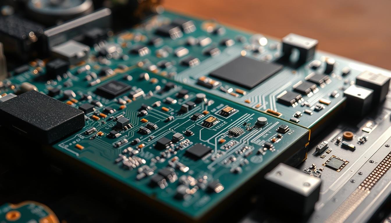
Signal Integrity and Electrical Performance
 showcasing the precise thickness of the board. The layers are meticulously depicted, with copper traces, dielectric materials, and protective solder mask visible. Warm, directional lighting highlights the intricate details, casting subtle shadows that accentuate the board's depth and texture. The image is captured at a slight angle, providing a visually engaging perspective that emphasizes the signal integrity and electrical performance characteristics of the pcb thickness.")
In electronics manufacturing, the thickness of a PCB is a critical factor that impacts its electrical performance and signal integrity. The dimensions of a PCB can significantly affect how signals are transmitted and received within electronic circuits. We must consider these factors when designing PCBs for various applications.
Impedance Control in Different Thickness Boards
Impedance control is crucial for maintaining signal integrity, especially in high-frequency applications. Thicker PCBs can offer better impedance control due to the increased distance between signal layers and ground planes. This allows designers to achieve the desired impedance characteristics more effectively. “The right PCB thickness is crucial for impedance control,” as it directly affects the signal quality.
Signal Propagation and Trace Characteristics
The thickness of a PCB influences signal propagation characteristics, including trace resistance, capacitance, and inductance. Thicker boards can have wider traces, reducing resistance and improving signal quality. However, they may also introduce additional capacitance and inductance if not properly designed. We leverage our expertise to optimize trace characteristics for various PCB thicknesses.
EMI Shielding Effectiveness
Thicker PCBs can provide better shielding against electromagnetic interference (EMI), which is critical for applications with sensitive components or circuits. By combining increased board thickness with proper ground plane design and layer stackup planning, we can significantly enhance EMI shielding effectiveness. Our testing has shown that increasing PCB thickness can provide 3-6 dB additional shielding effectiveness in many applications.
- EMI shielding effectiveness typically improves with increased board thickness, particularly when combined with proper ground plane design and strategic layer stackup planning.
- Thicker boards allow for more effective implementation of EMI mitigation techniques such as guard traces, stitching vias, and embedded shielding layers.
- The trade-off between board thickness and EMI shielding becomes particularly important in compact electronic devices where traditional shielding methods are limited.
Manufacturing Challenges with Non-Standard PCB Thickness
When it comes to PCBs with non-standard thickness, manufacturers face a range of challenges that can affect the overall quality and cost of the final product. The production process for these specialized boards requires careful consideration of various factors to ensure that the end product meets the required specifications.
Drilling and Hole Quality Issues
Drilling through non-standard thickness PCBs can be problematic due to the increased material that drill bits must penetrate. This can lead to issues with hole quality, including inaccurate hole placement, excessive wear on drill bits, and potential damage to the surrounding material. Specialized drilling techniques and equipment are often necessary to maintain precision and prevent damage.
Lamination and Etching Complexities
The lamination process for non-standard thickness PCBs can be more complex due to the need for precise control over pressure and temperature. This complexity can affect the uniformity of the laminate and the quality of the PCB. Additionally, etching processes may require adjustments to accommodate the varying thickness, ensuring that the desired circuit patterns are achieved accurately.
Assembly and Soldering Considerations
Assembly of non-standard thickness PCBs presents unique challenges, particularly during component placement and soldering. Thicker boards act as significant heat sinks, requiring modified thermal profiles with longer preheat stages and higher peak temperatures. Ensuring proper solder joint formation while preventing thermal damage is crucial. Our assembly processes include customized conveyor speeds and specialized fixtures to address these challenges.
By understanding and addressing these manufacturing challenges, we can ensure that PCBs with non-standard thickness meet the required quality and performance standards. Our expertise in handling such specialized PCBs enables us to provide high-quality solutions for complex electronics manufacturing needs.
PCB Thickness for Specific Applications
 of varying thicknesses, arranged neatly on a clean, reflective surface. The PCBs are labeled with the ESPCBA brand name, showcasing their precise dimensions and suitability for different electronic applications. The lighting is soft and diffused, highlighting the intricate copper traces and the subtle textures of the board materials. The scene conveys a sense of technical precision and expertise, inviting the viewer to explore the nuances of PCB thickness and its impact on PCBA performance and cost.")
In various electronic applications, the thickness of a PCB is a key consideration for designers and engineers. The optimal PCB thickness varies depending on the specific requirements of the application, including high-frequency, high-power, and compact portable devices.
High-Frequency and RF Applications
For high-frequency and RF applications, PCB thickness is critical for impedance control. A consistent thickness ensures that the signal transmission is not compromised. Typically, a thickness of 0.8mm to 1.6mm is preferred for these applications.
- Controlled impedance is crucial for signal integrity.
- Thickness consistency affects signal transmission quality.
High-Power Electronics Requirements
High-power electronics require PCBs that can handle increased thermal loads. Thicker PCBs with enhanced thermal conductivity are often used to dissipate heat effectively.
- Thermal management is critical in high-power applications.
- Thicker PCBs can provide better heat dissipation.
Compact and Portable Device Considerations
For compact and portable devices, thinner PCBs are preferred to minimize size and weight while maintaining necessary functionality. However, designers must balance the need for thinness with mechanical strength and thermal performance.
- Thinner PCBs (0.4mm-1.0mm) are used in compact devices.
- Designers must balance thinness with mechanical and thermal requirements.
How to Select the Optimal PCB Thickness
The choice of PCB thickness is crucial for balancing performance requirements and manufacturing constraints. Consulting with your PCB manufacturer during the design phase can help optimize production efficiency.
Balancing Performance Requirements
Effective collaboration with PCB manufacturers during the design phase is essential for optimizing thickness specifications. We recommend engaging manufacturers early to discuss thickness tolerances, material availability, and process capabilities before finalizing design specifications. This collaboration helps balance performance requirements with manufacturing capabilities.
Cost-Benefit Analysis
The relationship between design requirements and manufacturing constraints often reveals opportunities for minor thickness adjustments that can significantly improve manufacturability without compromising performance. By understanding the challenges associated with non-standard PCB thicknesses, designers can make informed decisions that balance performance and cost.
| Thickness Adjustment | Manufacturability Impact | Performance Impact |
|---|---|---|
| Minor Reduction | Improved manufacturability | Minimal performance impact |
| Minor Increase | Potential for increased cost | Possible performance enhancement |
Working with Manufacturers on Thickness Specifications
For projects with critical thickness requirements, we establish clear communication channels with manufacturers to ensure proper documentation of thickness specifications and verification methods. Manufacturers can provide valuable insights into thickness optimization based on their equipment capabilities and material supply chain, potentially identifying cost-saving alternatives that maintain required performance characteristics.
By working closely with PCB manufacturers and considering factors such as manufacturability, performance requirements, and cost-benefit analysis, designers can select the optimal PCB thickness for their projects.
Conclusion: Making Informed Decisions About PCB Thickness
In conclusion, selecting the appropriate PCB thickness is pivotal for achieving optimal performance, reliability, and cost in electronic devices. Throughout this guide, we’ve explored how thickness influences various aspects of PCBA performance and manufacturing costs, demonstrating its significance beyond mere mechanical specification.
We’ve seen that PCB thickness affects signal integrity, thermal management, and manufacturing complexity, making it a fundamental parameter in the design phase. The optimal thickness emerges from a thoughtful analysis of specific requirements, constraints, and priorities.
By understanding these factors, designers can make informed decisions, resulting in high-performance, reliable, and cost-effective electronic devices. We encourage designers to leverage these insights to balance immediate manufacturing considerations with long-term performance requirements.