Can a poorly designed PCB layout be the silent killer of your electronic device’s performance? The answer lies in understanding the crucial role of a ground plane in ensuring signal integrity and minimizing electromagnetic interference (EMI).
We design and manufacture PCBs where the concept of “ground” is not just about safety; it’s about creating a stable foundation for your electronic circuits. A well-designed ground plane is essential for reducing impedance and enhancing overall circuit performance.
A consistent ground plane serves as the backbone of proper PCB functionality, providing stability and protection against various electrical issues. As we explore the world of PCB design, we’ll examine how ground planes have evolved and why they’re more critical than ever in today’s high-speed, compact electronics.
Key Takeaways
- A consistent ground plane is crucial for signal integrity and minimizing EMI.
- Proper ground plane design reduces impedance and enhances circuit performance.
- Ground planes have evolved to become more critical in modern PCB design.
- A well-designed ground plane provides stability and protection against electrical issues.
- Understanding ground planes is essential for creating reliable electronic devices.
Understanding Ground Planes in PCB Design
A well-designed ground plane is essential for maintaining signal integrity and minimizing electromagnetic interference in PCBs. We will delve into the specifics of ground planes, exploring their definition, types, and roles in PCB design.
What Is a Ground Plane?
A ground plane in PCB design is a conductive layer that serves as the zero-voltage reference point for all components in the circuit. It is typically implemented as a copper layer within the PCB stackup, often covering entire layers to provide a low-impedance path for return currents. This design approach helps in reducing electromagnetic interference and ensuring signal integrity.
Types of PCB Ground Plane Connections
There are several types of ground plane connections, including signal ground, chassis ground, safety ground, and earth ground. Each type has its specific functions and applications. For instance, signal ground is used as a reference point for signal voltages, while chassis ground is connected to the metal enclosure of the device to provide shielding.
| Type of Ground | Function | Application |
|---|---|---|
| Signal Ground | Reference point for signal voltages | Signal processing circuits |
| Chassis Ground | Connected to the metal enclosure for shielding | Device enclosures |
| Safety Ground | Protects against electrical shock | Power distribution systems |
The Importance of a Consistent Ground Plane in Your PCB Layout
A well-designed ground plane is the backbone of a reliable PCB layout. We will explore the critical aspects that make a consistent ground plane indispensable in modern PCB design.
Providing a Stable Reference Voltage
A consistent ground plane ensures that all components on the PCB operate with the same voltage reference point, which is crucial for preventing voltage discrepancies that can lead to malfunction. By providing a stable reference voltage, a well-designed ground plane helps in maintaining the overall health of the circuit. This stability is particularly important in complex designs where multiple components interact.
Ensuring Signal Integrity
Signal integrity is directly impacted by the quality of the ground plane. A consistent ground plane minimizes noise and crosstalk, ensuring that high-speed signals maintain their integrity. This is achieved by providing a clear return path for signals, thus reducing electromagnetic interference and maintaining consistent impedance.
Minimizing Electromagnetic Interference
A well-designed ground plane plays a crucial role in minimizing electromagnetic interference (EMI). By providing a consistent ground, it reduces both emitted and received interference, thus ensuring that the PCB complies with EMC standards. Proper ground plane design is essential for reducing the risk of EMI-related issues.
| Aspect | Benefit of Consistent Ground Plane |
|---|---|
| Stable Reference Voltage | Prevents voltage discrepancies, ensuring all components operate correctly. |
| Signal Integrity | Minimizes noise and crosstalk, maintaining signal integrity. |
| Electromagnetic Interference | Reduces both emitted and received EMI, ensuring EMC compliance. |
Key Functions of Ground Planes in PCBs
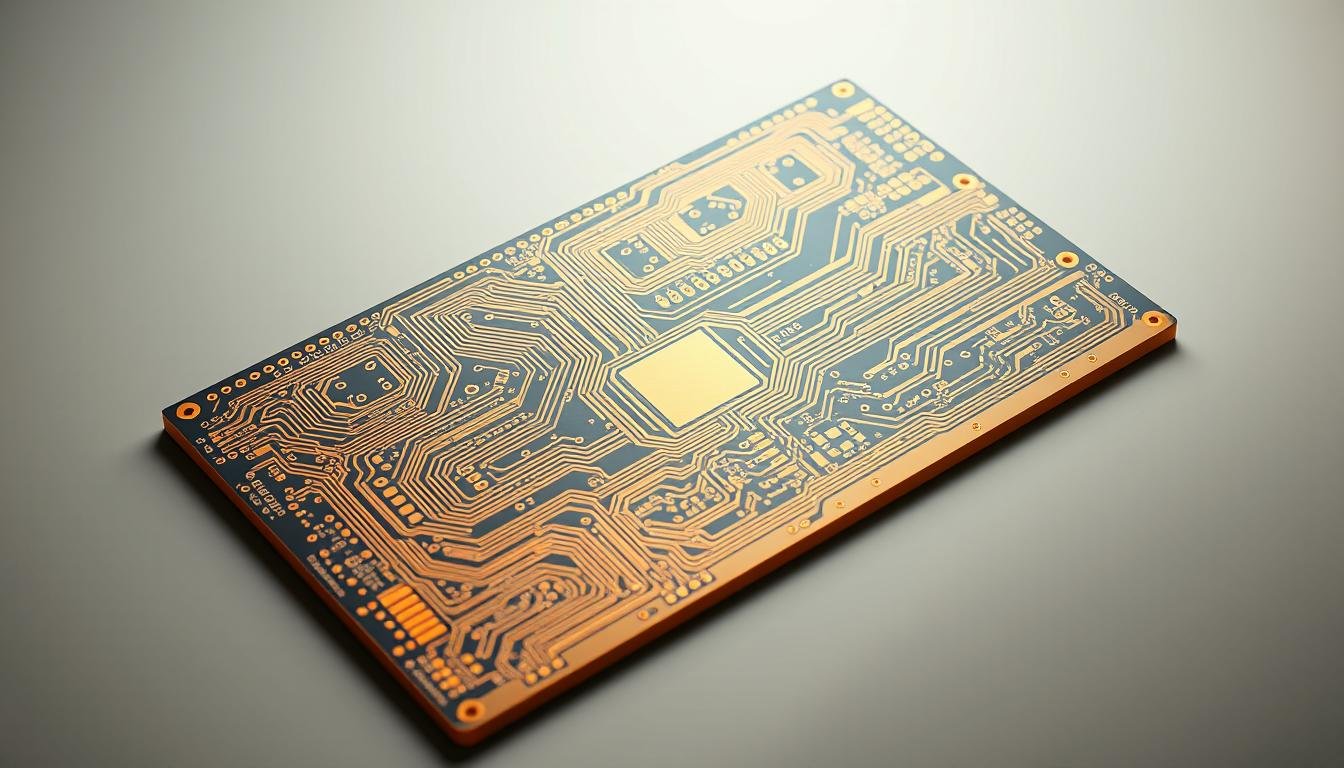
, showcasing the key functions and importance of a consistent ground plane. The scene features a cross-sectional view of the PCB, exposing the intricate copper traces, vias, and the prominent ground plane layer. The ground plane is rendered with a smooth, uniform metallic finish, contrasting with the surrounding circuit elements. Lighting is carefully placed to accentuate the layered structure, creating dramatic shadows and highlights that emphasize the ground plane's role in shielding and distributing power. The overall atmosphere is technical, precise, and educational, conveying the engineering principles behind ESPCBA's high-quality PCB design.")
Effective ground planes are the backbone of a well-designed PCB, facilitating signal integrity, power integrity, and shielding against electromagnetic interference. They are crucial for the reliability and performance of electronic circuits.
Effective Shielding
Ground planes provide effective shielding against electromagnetic interference (EMI), protecting sensitive components from external noise sources while containing internally generated EMI. This shielding is essential for maintaining the signal integrity of high-speed digital circuits.
Creating Signal Return Paths
The ground plane serves as a common return path for signals on the board. By providing a low-impedance path, it ensures that return currents can flow easily, minimizing the loop area and reducing EMI. This is critical for maintaining signal integrity in high-speed digital circuits.
Maintaining Power Integrity
Ground planes also contribute to power integrity by stabilizing voltage levels across the board. They provide low-inductance paths that help control noise, ensuring that power is delivered consistently to components. This is vital for the reliable operation of high-speed digital circuits.
| Function | Description | Benefit |
|---|---|---|
| Effective Shielding | Protects against EMI | Maintains signal integrity |
| Signal Return Paths | Low-impedance return path | Reduces EMI |
| Power Integrity | Stabilizes voltage levels | Ensures reliable operation |
Ground Plane Design Best Practices

To achieve optimal PCB performance, it’s vital to follow established ground plane design best practices. A well-designed ground plane is essential for maintaining signal integrity, minimizing electromagnetic interference, and ensuring the overall reliability of the PCB.
Maintaining Continuity in Ground Planes
Maintaining continuity in ground planes is critical for preserving low impedance and uninterrupted return paths. Avoiding cuts or splits in the ground plane ensures that the signal return paths are not disrupted, thereby reducing the risk of electromagnetic interference and signal degradation. Continuous ground planes also help in maintaining a stable reference voltage across the PCB.
Proper Via Placement and Stitching
Proper via placement and stitching techniques are vital for strengthening connections between ground planes across different layers. Strategic via positioning helps in creating a robust ground system by providing multiple paths for current to flow. This technique is particularly important in multilayer PCBs where ground planes are stacked between signal and power layers. Via stitching enhances the overall integrity of the ground plane by reducing inductance and improving shielding.
Layer Stackup Considerations
The layer stackup configuration plays a significant role in determining the performance of ground planes. Ideally, ground planes should be positioned adjacent to signal and power layers to provide effective shielding and minimize electromagnetic interference. A well-planned layer stackup ensures that the ground plane can effectively serve as a return path for signals and a sink for heat generated by power-intensive components.
Thermal Management Techniques
Ground planes can be effectively utilized for thermal management by designing them to dissipate heat from power-intensive components efficiently. By leveraging the thermal conductivity of the PCB material and the ground plane’s surface area, it’s possible to enhance heat dissipation and reduce the risk of overheating. This is particularly important in high-power applications where thermal management is critical for reliability.
Common Ground Plane Design Mistakes to Avoid
Even seasoned designers can fall into common traps when creating ground planes. Small oversights can result in significant problems, including increased noise and electromagnetic interference (EMI). We will explore these common mistakes and provide guidance on how to avoid them.
Fragmenting the Ground Plane
Fragmenting the ground plane is a critical mistake that can lead to increased noise and EMI problems. When the ground plane is split or cut, return currents are forced to take longer paths, resulting in increased impedance and noise. To avoid this, it’s essential to maintain a continuous ground plane whenever possible.
Routing Over Split Ground Planes
Routing signals over split ground planes can create impedance discontinuities and generate excessive EMI, potentially leading to compliance failures. It’s crucial to route signals over a continuous ground plane to maintain signal integrity. When this isn’t possible, using techniques like stitching capacitors can help mitigate the issues.
Improper Ground Connections
Improper ground connections, including insufficient grounding of components and poor via implementation, can lead to significant ground plane design issues. Ensuring that all components are properly grounded and that vias are correctly implemented is vital for maintaining the integrity of the ground plane.
By being aware of these common ground plane design mistakes, designers can take steps to avoid them, ensuring their PCBs perform as intended. As experts in PCB design, we emphasize the importance of careful ground plane design to maintain signal integrity and minimize EMI.
Ground Planes in Different PCB Applications
Effective ground plane design is critical in modern PCBs, supporting a wide range of applications from high-speed digital circuits to RF designs. The versatility of ground planes allows them to be adapted to various PCB types, each with its unique requirements and challenges.
High-Speed Digital Circuits
In high-speed digital circuits, ground planes are essential for managing timing and reducing jitter in fast-switching signals. Components like processors, memory modules, and FPGAs rely heavily on well-designed ground planes to maintain signal integrity. By providing a stable reference voltage and minimizing electromagnetic interference, ground planes help ensure the reliable operation of high-speed digital systems.
RF and Microwave Designs
For RF and microwave designs, ground planes often function as part of the transmission system, directly impacting signal performance. Proper ground plane design in these applications is crucial for maintaining impedance control and minimizing signal loss. Techniques such as via stitching and careful layer stackup planning are employed to optimize ground plane performance in RF and microwave PCBs.
Mixed-Signal Systems
In mixed-signal systems, where analog and digital circuits coexist, ground plane design becomes particularly challenging. It’s essential to isolate sensitive analog circuits from noisy digital circuits while maintaining a continuous ground plane. Techniques like split ground planes or careful routing can help minimize crosstalk and ensure system reliability. For more insights on managing ground planes in complex systems, visit our article on ground planes in PCBs.
Conclusion
The significance of a consistent ground plane cannot be overstated in the context of PCB design and manufacturing. As we’ve discussed, a well-implemented ground plane is crucial for signal integrity, minimizing electromagnetic interference (EMI), and ensuring overall performance and reliability of the electronic device.
Proper ground plane implementation offers numerous benefits, including improved signal integrity, reduced EMI, better thermal management, and enhanced overall reliability. By avoiding common ground plane design mistakes, designers can save significant time and cost during the development and testing phases of PCB production.
Collaborating with experienced PCB manufacturers like VSE can provide valuable guidance on ground plane design best practices specific to your application. With over forty years of experience in building life-saving and life-changing devices, we understand the importance of a well-designed ground plane in achieving optimal PCB performance.
As electronic systems become increasingly complex, the importance of a consistent ground plane will only continue to grow. By prioritizing ground plane design and leveraging the expertise of seasoned PCB manufacturers, designers can ensure the reliability and performance of their electronic devices.