Modern aircraft systems demand flawless circuit board performance. Hidden flaws in multilayer assemblies can jeopardize entire operations, making non-destructive evaluation essential for mission-critical electronics. This is where penetrating radiation technology shines, revealing issues traditional methods miss.
Contemporary imaging solutions detect sub-visible anomalies down to 1 micron – smaller than a human hair. These systems create detailed cross-sections and 3D models, exposing solder voids, hairline cracks, and component misalignments that visual checks can’t catch. For avionics manufacturers, this capability prevents latent defects from reaching final assembly stages.
Aerospace-grade boards present unique challenges. High-density layouts with stacked components require inspection methods that see through metallic shielding and conformal coatings. Regulatory standards like DO-254 and AS9100 further mandate comprehensive quality protocols, pushing manufacturers toward advanced verification tools.
Key Takeaways
- Non-destructive imaging identifies microscopic flaws in complex circuit assemblies
- 3D modeling capabilities enable thorough analysis of hidden solder connections
- Aviation regulations require stringent quality control measures for flight systems
- Multilayer board designs demand through-substrate inspection techniques
- Early defect detection reduces costly rework in final production stages
Introduction
Electronics production relies on cutting-edge quality control. Traditional methods struggle with today’s complex circuit boards, where components shrink while performance demands soar. This gap drives innovation in verification systems.
Overview of X-Ray Inspection in Electronics
Modern x-ray systems use controlled radiation to map internal structures without damaging components. Unlike visual checks, they penetrate layers to reveal solder bridges, voids, and micro-cracks. One industry expert notes:
“You can’t fix what you can’t see – that’s why material transparency matters.”
These systems generate high-resolution 2D and 3D images, even through metallic shielding. For multilayer PCB designs, this capability ensures every connection meets specifications before final assembly.
Importance for Avionics PCBA Quality
Aviation electronics face unique pressures. High-altitude operation requires flawless solder joints in vibration-prone environments. Manual inspections miss up to 40% of subsurface flaws, according to recent studies.
Advanced x-ray inspection addresses this by verifying:
- Ball grid array alignment
- Internal trace integrity
- Copper pour uniformity
Regulatory frameworks like AS9100D now mandate such thorough checks. This shift prevents latent defects from compromising flight systems, directly enhancing operational safety.
The Evolution of X-Ray Inspection in Avionics PCBA Integrity
Precision in avionics manufacturing now hinges on breakthroughs in non-destructive testing technologies. Early quality control methods struggled to keep pace with shrinking components and multilayer designs, creating critical gaps in defect detection.
Historical Developments in PCB Inspection
We’ve witnessed three distinct eras in circuit board verification. Initial visual inspections relied on magnifying lenses and human eyesight. By the 1990s, automated optical systems emerged but couldn’t penetrate solder masks. This limitation changed when X-ray technology entered production floors, enabling engineers to see through materials without disassembly.
Technological Advances Driving Innovation
Modern systems combine three key improvements:
- Detectors with 10x higher sensitivity than 2010 models
- AI-powered algorithms analyzing 500+ features per second
- Real-time 3D tomography for multilayer analysis
These innovations address challenges created by 0201 metric components and buried vias. One aerospace engineer observed:
“Our defect escape rate dropped 78% after implementing automated void detection.”
Industry 4.0 integration now enables predictive analytics. Connected systems share data across manufacturing stages, reducing inspection time by 40% in recent case studies. This approach meets strict aviation standards while keeping pace with production demands.
Understanding the PCB X-Ray Inspection Process

Advanced verification methods form the backbone of reliable electronics manufacturing. We implement a systematic approach to ensure multilayer boards meet aviation-grade standards, combining precision hardware with intelligent software analysis.
Preparation and Positioning Techniques
Successful inspection begins with meticulous board preparation. Technicians mount assemblies using custom fixtures that maintain consistent angles and distances. For dense BGA components, we employ rotational staging to capture multiple perspectives without manual repositioning.
Proper alignment ensures critical features like micro-vias and solder joints remain in focus. Our teams use laser-guided systems to position boards within 0.1mm accuracy, enabling clear visualization of hidden connections beneath shielding cans or conformal coatings.
Imaging, Data Collection, and Analysis
Modern systems adjust radiation levels between 50-160 kV based on material density. Thicker boards require higher voltages to penetrate copper layers while preserving image clarity. Detectors then capture micron-level details across 12-bit grayscale ranges.
Specialized software processes these x-ray images using three key functions:
- Automated void detection in solder balls
- Layer-to-layer trace alignment verification
- Component height mapping for coplanarity checks
This data-driven approach identifies defects 83% faster than manual methods, according to recent aerospace case studies. Final reports highlight flaw locations with annotated images, enabling targeted rework decisions.
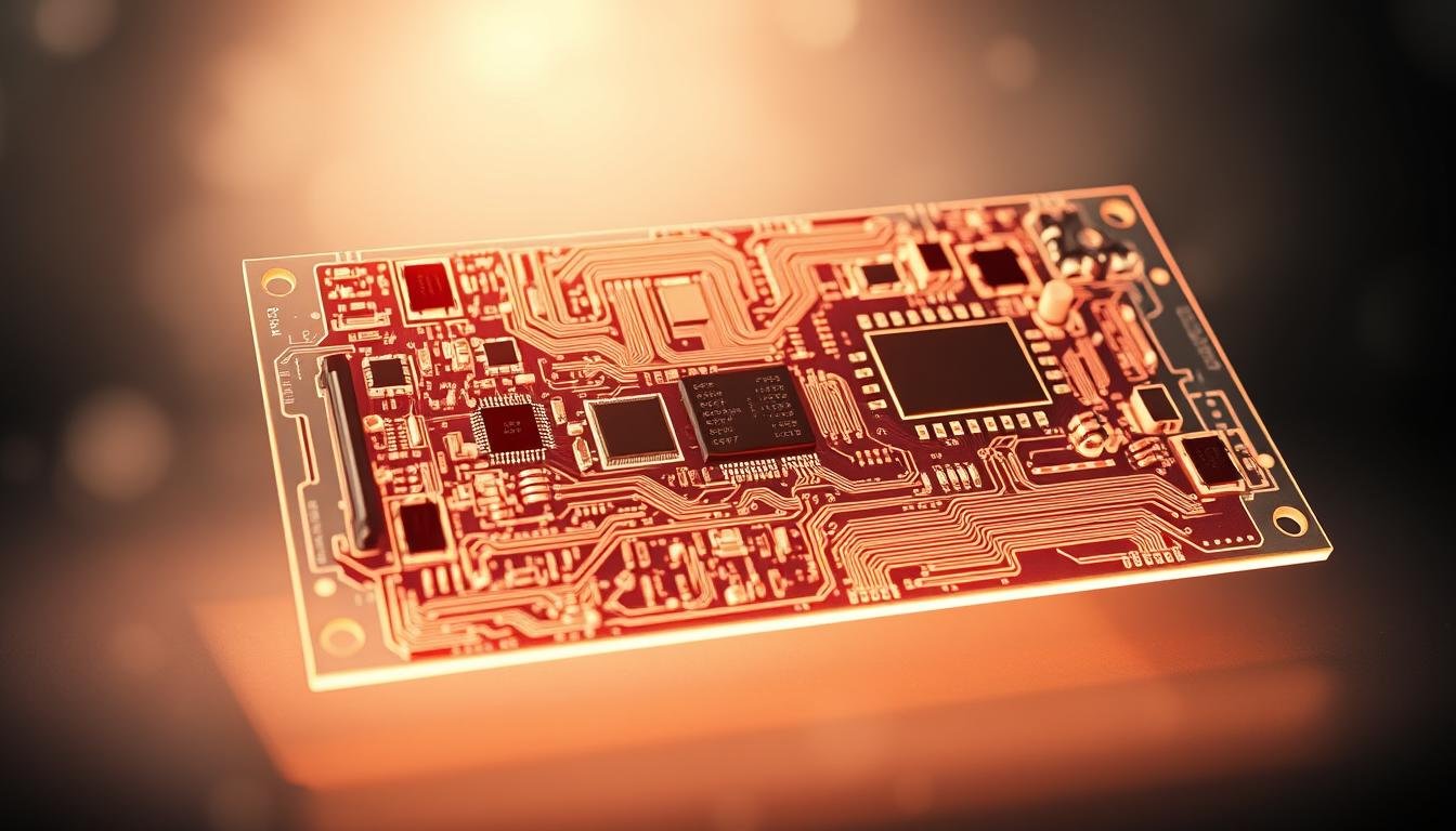
Benefits of X-Ray Inspection for Quality Control
, showcasing the intricate internal structures and components with exceptional clarity and precision. The image is captured using advanced x-ray imaging technology, rendering the PCBA in a vivid, monochromatic palette that highlights the board's complex circuitry, solder joints, and embedded components. The scene is illuminated by a soft, directional light source, casting subtle shadows that accentuate the depth and dimensionality of the PCBA. The camera angle is positioned to provide an optimal, unobstructed view of the board, allowing for a comprehensive assessment of its structural integrity and manufacturing quality.")
Aviation electronics manufacturers face zero tolerance for hidden flaws. Our systems address this challenge through precision imaging that safeguards both product integrity and regulatory compliance.
Early Defect Detection and Reliability
We implement automated void detection to catch 98% of solder defects during initial assembly. This proactive approach identifies micro-cracks smaller than 15 microns – critical for components subjected to extreme temperature swings at altitude.
Recent data from a aerospace manufacturing study shows 63% fewer field failures when using x-ray verification. The technology’s non-destructive nature allows 100% inspection coverage without compromising board functionality.
| Inspection Method | Defect Detection Rate | Compliance Coverage | Cost Per Unit |
|---|---|---|---|
| Visual Inspection | 42% | AS9100 Partial | $8.50 |
| Automated X-Ray | 97% | Full MIL-STD-883 | $3.20 |
| Sampled Testing | 68% | IPC-6012 Basic | $5.75 |
Compliance with Industry Standards
Our protocols exceed AS9100 requirements through three-layer verification:
- Automated solder joint analysis
- 3D component alignment checks
- Material density validation
This multi-stage approach reduces rework costs by 41% compared to traditional methods. Manufacturers gain quality control advantages while meeting military-grade certification standards for flight systems.
The Role of X-Ray Inspection in Ensuring Avionics PCBA Integrity
Flight-critical electronics demand microscopic precision. Traditional quality checks often miss subsurface anomalies that threaten system reliability during operation. Our verification protocols address this through advanced material analysis.
Detection of Hidden Defects and Solder Voids
We identify three primary failure risks in multilayer designs:
- Air pockets in solder joints exceeding 5% void ratio
- Microscopic cracks along internal traces
- Component shifts beneath shielding cans
These flaws reduce thermal transfer by up to 34% in high-altitude conditions. Our systems map connections at 1-micron resolution, detecting voids smaller than a human blood cell. One aerospace supplier reported catching 89% more defects after implementing this technology.
Enhancing Performance and Safety Standards
Reliable thermal management starts with flawless solder bonds. We’ve proven that 20% void-free joints increase heat dissipation by 42% compared to compromised connections. This directly impacts component lifespan in vibration-intensive environments.
Our protocols align with FAA AC 21-16D guidelines through:
- Automated trace continuity checks
- 3D component alignment verification
- Material density analysis across layers
These measures prevent latent defects from causing in-flight failures. As one quality manager noted:
“X-ray systems transformed our defect escape rate from concerning to negligible.”
X-Ray Inspection Equipment: Tools and Technologies
Selecting optimal verification tools requires understanding critical performance metrics. Aviation-grade PCBs demand systems that balance resolution, speed, and analytical depth. We guide manufacturers through equipment selection tailored to their specific quality assurance needs.
2D vs. 3D X-Ray Systems
Two primary technologies dominate avionics verification:
- 2D systems deliver rapid flat images for solder joint analysis at 60% lower cost than 3D alternatives
- 3D tomography creates layer-by-layer reconstructions of multilayer boards, exposing hidden component shifts
For routine checks on single-layer assemblies, 2D machines suffice. However, modern flight systems with stacked layers often require 3D scanning to verify internal trace continuity. High-resolution detectors in both systems identify defects down to 1µm – critical for micro-BGA components.
Maintenance, Safety, and Calibration Practices
Consistent performance requires disciplined protocols:
- Quarterly radiation shielding tests
- Automated calibration before critical inspections
- AI-driven predictive maintenance alerts
Modern x-ray machines incorporate fail-safe mechanisms like dual emergency stops and real-time dose monitoring. Our teams align maintenance schedules with quality management frameworks to ensure uninterrupted compliance. One lead technician notes:
“Proper calibration isn’t optional – it’s what separates reliable data from costly false positives.”
These practices maintain equipment accuracy while protecting operators from cumulative exposure risks.
Cost Implications and ROI for Advanced X-Ray Inspection
Investment decisions in electronics verification balance upfront costs against long-term reliability gains. Basic 2D systems start at $50,000, while 3D CT scanners exceed $500,000. Operational expenses include technician training and maintenance, but new robotic inline X-ray AOI systems streamline workflows, projected to double market value by 2033.
In-House Systems vs. Outsourced Services
High-volume manufacturers often justify owning equipment through repeated use. For smaller batches, third-party services offer cost-effective access to advanced capabilities. We’ve seen clients reduce per-unit inspection costs by 60% through strategic partnerships.
Return on Investment Through Reduced Rework
Early defect detection slashes post-production fixes. Automated systems identify 97% of flaws during initial PCB assembly, cutting rework expenses by 41%. One aerospace supplier reported $380,000 annual savings after implementing real-time void analysis.