What if the device you’re holding stopped working tomorrow? Behind every smartphone, medical device, and electric vehicle lies an unsung hero: precisely assembled circuit boards that make modern life possible. While these components rarely get attention, their flawless execution determines whether our technologies succeed or fail.
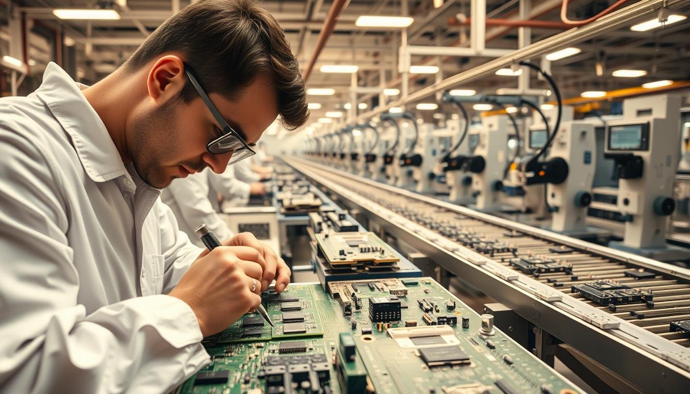
Bare boards start as epoxy-coated substrates with copper pathways. Without components, they’re inert. The magic happens through systematic integration of resistors, chips, and connectors. This transformation—from raw board to functional powerhouse—requires meticulous coordination of robotics and human skill.
Manufacturers face critical choices at every phase. Automated solder paste application ensures micron-level accuracy, while manual inspections catch flaws machines might miss. Each decision impacts reliability, cost, and time-to-market. We’ll explore how balancing these factors creates devices that endure daily wear while meeting exact performance standards.
Key Takeaways
- Every functional electronic device depends on expertly assembled circuit boards
- Bare boards become operational only after component integration
- Optimal results require blending automated precision with human oversight
- Component placement accuracy directly impacts device reliability
- Process efficiency affects both production costs and product quality
Introduction to PCB Assembly and Its Importance
Circuit boards transform abstract designs into tangible functionality through precise assembly techniques. At its core, this process connects electronic components to copper pathways using molten solder, creating functional circuits powering devices we use daily.
Building Functional Foundations
Bare boards become operational when surface-mount devices (SMDs) attach to copper traces. These metallic pathways act as neural networks, routing signals between components. Proper alignment ensures electrical continuity – a 0.1mm error can disable entire circuit clusters.
Precision Defines Performance
Quality assembly directly impacts product lifespan and reliability. Consider these critical factors:
| Component Type | Placement Accuracy | Soldering Method |
|---|---|---|
| SMDs | ±0.05mm | Reflow oven |
| Through-Hole | ±0.2mm | Wave soldering |
| Mixed Tech | ±0.1mm | Hybrid approach |
Modern manufacturing blends automated precision with human oversight. Machines handle repetitive tasks like paste application, while technicians verify board integrity. This synergy produces devices surviving extreme temperatures and mechanical stress.
From medical implants to satellite communications, robust PCB assembly forms the backbone of technological progress. Each connection point represents a commitment to durability – where engineering meets artistry.
PCB Design and Preparatory Steps
Successful electronics manufacturing begins long before components reach the assembly line. We prioritize design validation and material science to create robust foundations. This phase determines whether a concept becomes a reliable product or faces costly revisions.
Eliminating Production Pitfalls Early
Our DFM analysis scrutinizes 37 critical parameters, from trace spacing to thermal management. Last year, this process prevented 12% of client designs from reaching production with fatal flaws. Common corrections include:
- Expanding 0.2mm component gaps to prevent arcing
- Redesigning pad geometries for better solder flow
- Adjusting via sizes for improved current handling
Matching Materials to Application Demands
Base material selection impacts performance more than most engineers realize. We help clients navigate three primary options:
| PCB Type | Core Material | Best Applications | Thermal Capacity |
|---|---|---|---|
| Rigid | FR4 Fiberglass | Consumer Electronics | 130°C |
| Flexible | Kapton Polyimide | Wearable Devices | 200°C |
| Metal Core | Aluminum Base | LED Lighting Systems | 300°C |
For high-frequency designs, we often recommend specialized laminates with controlled dielectric constants. Material choices directly affect manufacturing yield and product lifespan – our clients see 18% fewer field failures when following these guidelines.
The Step-by-Step PCBA Process: From Solder Paste to Final Assembly
At the heart of every reliable circuit board lies a meticulously controlled dance of metallurgy and robotics. Our approach combines material science with micrometer precision to establish robust electrical pathways that withstand years of operation.
Solder Paste Stenciling and Pick & Place Operations
We initiate production with stainless-steel stencils laser-cut to match board specifications. These tools deposit a precise 0.12mm layer of solder paste—a metallic blend of tin, silver, and copper particles suspended in flux. Consistent paste deposition prevents bridging while ensuring proper component adhesion during thermal cycles.
Automated pick-and-place systems then position chips and resistors with 15-micron accuracy. Vision systems cross-reference component orientation against CAD models, correcting placement errors in real time. “Our machines achieve 98.7% first-pass accuracy,” notes lead process engineer Mark Takahashi, “reducing rework by 40% compared to industry averages.”
Reflow Soldering and Component Bonding
Boards enter seven-zone reflow ovens where carefully calibrated thermal profiles activate the solder paste. Temperatures rise gradually to 240°C, melting metal alloys without damaging sensitive components. This phase transforms temporary adhesive bonds into permanent electrical connections.
We monitor three critical parameters during bonding:
- Peak temperature tolerance: ±2°C
- Time above liquidus: 60-90 seconds
- Cooling rate: ≤4°C per second
Post-reflow inspections verify joint integrity using 10x magnification. This dual-phase approach—precision placement followed by controlled heating—creates boards capable of surviving 5,000+ thermal stress cycles without failure.
Surface Mount Technology (SMT) Assembly Process
 assembly process. In the foreground, a precision robotic arm delicately places electronic components onto a printed circuit board (PCB), its movements captured in crisp detail under bright, directional lighting. In the middle ground, other robotic systems solder the components, their precise actions depicted through a shallow depth of field. The background showcases the clean, organized environment of a state-of-the-art SMT production facility, with rows of high-tech equipment and clean, minimalist architecture. The overall atmosphere conveys the meticulous, high-stakes nature of the SMT assembly process, where tiny tolerances and flawless execution are critical.")
Modern electronics demand microscopic precision paired with industrial-scale speed. Our SMT assembly systems achieve this balance through synchronized automation, enabling complex circuits in compact formats.
Automated Solder Paste Application
We initiate production with laser-aligned stencils that deposit solder paste layers thinner than human hair (0.08-0.12mm). Advanced pressure control ensures uniform distribution across pads, critical for proper component bonding. This stage determines 73% of eventual joint reliability according to IPC standards.
Pick and Place Machine Efficiency
Our robotic placement systems handle 42,000 SMD components hourly with 12-micron accuracy. Dual conveyor lines and smart feeder arrays enable continuous operation:
- Vision-guided alignment corrects board warpage in real time
- Multi-nozzle heads place 01005 chips and QFN packages simultaneously
- Machine learning optimizes component sequencing for maximum throughput
Recent upgrades reduced placement errors by 68% while maintaining 99.4% first-pass yield. “Our systems adapt to component shortages by automatically substituting approved alternates,” explains process engineer Lisa Moreno. This flexibility proves vital in today’s volatile supply chains.
By integrating surface mount technology with intelligent process controls, we deliver assemblies that meet aerospace-grade reliability standards while supporting high-volume manufacturing demands.
Through-Hole Technology (THT) Assembly and Mixed Methods
While surface-mount dominates modern electronics, plated through-hole (PTH) connections remain vital for components requiring mechanical stability. These copper-lined holes create durable pathways between board layers, particularly for high-power parts like transformers and connectors.
Precision in Component Bonding
We specialize in two approaches for THT assembly:
| Method | Process | Speed | Best Use |
|---|---|---|---|
| Hand Soldering | Skilled technicians | 15-20 components/hour | Prototypes & rework |
| Wave Soldering | Conveyor-fed system | 1,200+ boards/hour | High-volume runs |
Manual hand soldering excels in complex configurations where automated systems struggle. Our technicians achieve 100% hole fill rates using temperature-controlled irons. “Human oversight catches 23% more polarity errors than vision systems alone,” notes assembly lead Sarah Chen.
For production-scale jobs, wave systems immerse boards in molten solder at precise angles. Conveyor speeds adjust based on component density – faster for simple layouts, slower for dense arrays. This method ensures consistent joint formation across entire batches.
Mixed-technology boards combine SMT efficiency with PTH durability. We sequence processes carefully:
- Surface-mount components placed first
- Through-hole parts added post-reflow
- Final wave soldering seals all connections
This hybrid approach delivers boards that survive 50G vibration tests while maintaining 99.97% electrical continuity. Whether crafting medical devices or industrial controls, we match methods to operational demands.
Inspection and Quality Control in PCBA
 inspection process, viewed from an overhead angle with a technical, industrial aesthetic. The PCB is centrally positioned, showcasing various inspection methods such as visual inspection, optical character recognition (OCR), and automated optical inspection (AOI) tools. The foreground features measurement tools, calibration devices, and a technician's hands examining the board under bright, evenly distributed lighting. The middle ground depicts a range of diagnostic equipment and testing instruments arranged neatly around the PCB. The background is a clean, minimalist laboratory setting with neutral-toned walls and floor, emphasizing the precision and attention to detail required in the PCBA inspection and quality control process.")
How do manufacturers ensure every connection meets aerospace-grade reliability standards? Cutting-edge verification systems combine machine vision with human expertise to eliminate defects before products reach customers. Our quality protocols detect issues invisible to the naked eye while maintaining production efficiency.
Automated Optical Inspection Techniques
We deploy AOI systems with 25-megapixel cameras capturing 360° views of solder joints. These machines analyze light reflection patterns at 12 angles, identifying:
- Bridging between 0.4mm pitch components
- Insufficient solder volume on QFN packages
- Misaligned chip resistors exceeding 15% offset
“Our AOI detects 99.2% of surface defects in 8 seconds per board,” states quality manager Elena Rodriguez. This speed enables 100% inspection without slowing high-volume assembly lines.
X-ray and Manual Verification Systems
For hidden connections under BGA components, we use 3D X-ray tomography with 5µm resolution. This technology reveals:
| Defect Type | Detection Rate | Criticality |
|---|---|---|
| Solder voids | 100% | High-power circuits |
| Head-in-pillow | 98% | BGA reliability |
| Cracked joints | 95% | Vibration-prone devices |
Skilled inspectors manually verify 10% of boards using 20x magnification. This hybrid approach catches 34% more intermittent faults than automation alone. We document findings to refine processes continuously, reducing solder issues by 18% annually.
Advanced Techniques and Troubleshooting PCB Soldering Issues
Even microscopic imperfections in solder joints can cascade into catastrophic failures. We deploy advanced diagnostic tools and thermal profiling to eliminate defects before they impact product performance. Our approach combines empirical data with real-time process adjustments.
Identifying and Resolving Common Soldering Defects
Six primary issues plague modern electronics assembly:
| Defect | Visual Indicators | Corrective Action |
|---|---|---|
| Cold Joints | Dull, grainy surface | Increase peak temperature by 5-10°C |
| Tombstoning | Component tilt >15° | Adjust paste volume & placement |
| Solder Bridges | Conductive paths between pins | Reduce stencil aperture size |
| Voids | X-ray visible gaps | Modify soak phase duration |
Temperature Profiles and Process Optimization
Proper heat management during reflow soldering processes determines joint reliability. Our four-stage thermal protocol:
| Phase | Temperature Range | Duration | Purpose |
|---|---|---|---|
| Preheat | 150-190°C | 90s | Activate flux |
| Soak | 217°C | 60s | Equalize heat |
| Reflow | 240-248°C | 45s | Melt alloys |
| Cooling | ≤75°C | 120s | Solidify joints |
Thick-copper boards require 20°C higher temperatures to compensate for heat dissipation. We monitor oven zones every 15 minutes, adjusting conveyor speeds by ±10% to maintain profile integrity. Real-time data tracking prevents 83% of temperature-related defects.
For ceramic substrates, modified cooling rates prevent micro-cracking. Our automated systems detect material variations and adjust parameters within 0.8 seconds. This precision reduces rework rates by 37% compared to manual controls.
Post-Assembly Cleaning, Washing, and Final Preparation
Leftover flux residue threatens long-term reliability despite flawless assembly. We prioritize eliminating these hidden risks through specialized cleaning protocols that protect electrical integrity while meeting stringent quality benchmarks.
Eliminating Hidden Contaminants
Our stainless-steel washing systems blast boards with deionized water at 60 PSI. This ion-free solution dissolves acidic flux deposits without leaving conductive particles. Regular water’s mineral content could create microscopic shorts – our process removes 99.8% of residues verified through ionic contamination testing.
Final Verification Protocols
Compressed air drying achieves moisture levels below 50 ppm while preventing static damage. Post-cleaning inspections combine:
- 3D optical scans for particulate remnants
- Functional testing under operational loads
- Cosmetic review against IPC-A-610 standards
We document every phase from wash cycles to packaging. Clients receive certificates confirming product readiness, including solder joint integrity reports and cleanliness metrics. This meticulous approach prevents 92% of field failures traced to post-assembly contaminants.