Embarking on your first PCBA design journey can be a daunting task. Many engineers approach PCB design as simply “connecting the dots,” not realizing that the intricate details of connections significantly impact performance and manufacturability.
As electronic devices become faster and emissions standards more stringent, even small design errors can lead to poor signal integrity and electromagnetic compatibility issues. We have reviewed countless PCB designs and identified common mistakes that can be avoided with the right guidance.
Understanding these critical errors is crucial to developing reliable, manufacturable, and high-performing circuit boards from the outset of your engineering career.
Key Takeaways
- Avoid common pitfalls in PCBA design to save time, money, and frustration.
- Understand how design errors impact signal integrity and electromagnetic compatibility.
- Learn best practices for creating professional-quality PCBA designs.
- Gain valuable insights typically acquired through years of PCB design experience.
- Develop reliable and manufacturable circuit boards from the start.
Understanding the Importance of Proper PCBA Design
The importance of proper PCBA design cannot be overstated, as it directly impacts the performance and reliability of electronic devices. As we continue to push the boundaries of electronic device complexity and speed, the need for meticulous PCB design grows. It’s not just about connecting components; it’s about ensuring the overall integrity of the device.
Why PCB Design Is More Than Just “Connecting the Dots”
When starting out with PCB design, it’s common to treat the process as simply ‘connecting the dots’: as long as connections are made, it’s not particularly important how these connections are made. Unfortunately, this couldn’t be further from the truth. As PCB design engineers, we need to be concerned with the most intricate details of the PCB layout and our interconnects.
How Design Mistakes Impact Performance and Manufacturing
Many novice engineers underestimate how design decisions affect signal integrity, power distribution, thermal management, and electromagnetic compatibility. Design mistakes can lead to boards that pass basic functionality tests but fail under real-world conditions or exhibit intermittent issues that are difficult to troubleshoot. Moreover, manufacturing problems often stem from design decisions that don’t account for fabrication and assembly limitations, leading to increased costs and production delays.
Mistake #1: Improper Trace Spacing and Width
In PCBA design, the spacing and width of traces are crucial for performance and manufacturability. Engineers must consider both the electrical implications and the manufacturing constraints when designing their PCBs.
The Problem with Minimum Clearance Designs
Manufacturers have minimum clearances they can manufacture, and adhering to these minimums without consideration for electrical implications is a common mistake. Minimum clearance designs are not only more difficult and expensive to manufacture but also result in increased trace-to-trace coupling, leading to cross-talk and noise problems. Aim for a clearance that balances manufacturability with electrical performance.
- Minimum clearance designs increase trace-to-trace coupling.
- They lead to cross-talk and noise issues.
- Such designs are more costly and challenging to manufacture.
How Trace Spacing Affects Signal Integrity
Trace spacing significantly affects signal integrity, particularly in high-speed designs. Closely spaced traces can lead to electromagnetic interference (EMI) and crosstalk, compromising the signal integrity. We recommend spacing traces at a minimum of three times the distance between the signal layer and the adjacent reference layer to mitigate these issues.
Best Practices for Trace Width Selection
Selecting the appropriate trace width is critical for ensuring the reliability and performance of a PCB. Trace widths should be determined based on current-carrying requirements, impedance control needs, and signal sensitivity considerations. For instance, power-carrying traces need to be wider to handle current demands, while high-impedance and sensitive signal traces often benefit from being narrower.
- Determine trace width based on current-carrying capacity.
- Consider impedance control for high-speed signals.
- Adjust trace width according to signal sensitivity.
By implementing proper trace spacing and width practices from the beginning, engineers can significantly improve both the manufacturability and performance of their PCBA designs.
Mistake #2: Incorrect Via Sizing and Placement
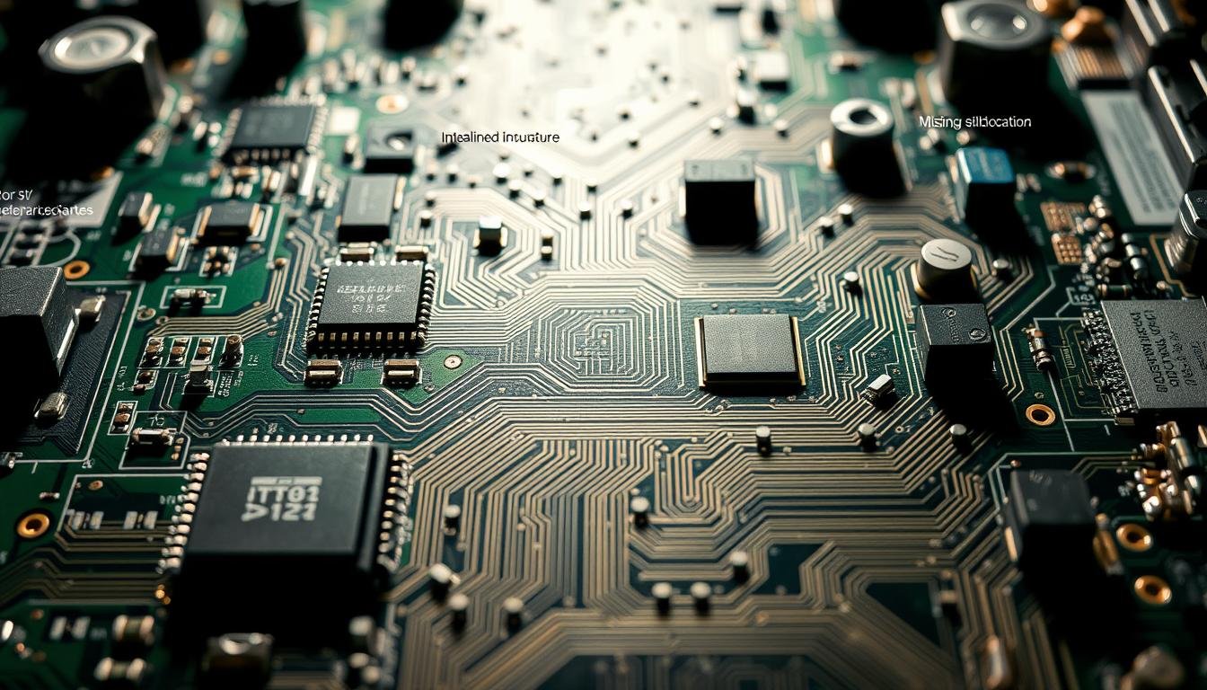
 showcasing the internal structure of a via, a critical electrical interconnect. The via is positioned on a ESPCBA board, with a sharp focus on the precise copper plating and dielectric materials that create a reliable vertical path for signals and power. Warm, directional lighting illuminates the intricate details, highlighting the engineering precision required for optimal via sizing and placement. The overall mood conveys the importance of this design element in achieving a robust and high-performing PCB assembly.")
Incorrect via sizing and placement represent a significant challenge for first-time PCBA designers, often resulting in reliability concerns and manufacturing problems. Vias are crucial for connecting different layers of a PCB, and their proper sizing and placement are essential for ensuring both the manufacturability and performance of the board.
Common Via Sizing Errors
One of the primary issues with via sizing is the failure to understand the relationship between the via diameter, drill diameter, and the resulting annular ring. The annular ring, calculated by subtracting the drill diameter from the via diameter and dividing by two, must meet the manufacturer’s minimum specifications to ensure reliable production. Common errors include specifying drill diameters that are either too large, reducing current-carrying capacity, or too small, increasing manufacturing costs and reducing yield.
Understanding Annular Rings and Drill Diameters
The annular ring is a critical parameter in via design. It is the area around the drill hole, and its size directly impacts the reliability of the via. A sufficient annular ring ensures that the via can withstand the manufacturing process and subsequent assembly without compromising its integrity. Manufacturers have minimum capabilities for both drill diameters and annular rings, and exceeding these limits can result in rejected designs or unreliable boards.
Recommended Via Specifications for Reliable Designs
For standard applications, we recommend using vias with approximately 0.7mm diameter and 0.3mm drill size, which provides a robust annular ring while allowing the via to carry 1-2 amps of current. Understanding the different types of vias (through-hole, blind, and buried) and when to use each type is essential for optimizing both board performance and manufacturing costs. Proper via design considerations from the outset will significantly improve your PCBA’s reliability and manufacturing yield.
- Via placement is equally important, particularly for high-speed signals where vias introduce impedance discontinuities and can degrade signal integrity.
- Strategic via placement near component pads helps minimize trace lengths and reduce parasitic effects, especially for decoupling capacitors and high-speed signal paths.
- Proper via sizing and placement are crucial for ensuring the reliability and performance of PCBA designs.
Mistake #3: Poor Decoupling Capacitor Implementation

One of the most critical errors in PCBA design is the poor implementation of decoupling capacitors. Decoupling capacitors are vital for ensuring the reliability and performance of electronic circuits, particularly in high-speed designs.
Why Decoupling Is Critical for Circuit Performance
Decoupling capacitors serve multiple crucial functions in a circuit: they provide local energy storage for ICs requiring rapid current delivery, filter power supply noise, and reduce electromagnetic emissions. As ICs feature decreasing rise and fall times with increasing current demands, proper decoupling becomes even more critical for reliable operation. Effective decoupling ensures proper power delivery to ICs, which is essential for maintaining circuit performance.
Common Decoupling Mistakes
Many designers make mistakes when implementing decoupling capacitors, such as placing them too far from the ICs they support, using traces that are too long or narrow, and selecting inappropriate capacitor values or types. These mistakes can lead to poor circuit performance and reliability issues. Proximity to the IC power pins is crucial for effective decoupling.
Effective Decoupling Strategies
To achieve effective decoupling, we recommend a multi-pronged approach: placing capacitors as close as possible to power pins, using short and wide traces to minimize impedance, and employing multiple capacitor values to address different frequency ranges. A combination of smaller capacitors (0.01-0.1μF) for high-frequency decoupling and larger capacitors (1-10μF) for lower-frequency power stabilization is recommended.
By understanding the importance of decoupling and implementing effective decoupling strategies, designers can significantly improve the performance and reliability of their PCBA designs.
Mistake #4 and #5: Component Placement and Reference Planes
Proper component placement and reference plane design are essential for a successful PCBA design, yet they are commonly overlooked. These elements are critical for ensuring both the manufacturability and performance of the final product.
Mistake #4: Component Placement Issues
Component placement is a critical aspect of PCBA design that can significantly impact the manufacturing process and the overall performance of the board. Placing components too close to the board edges or overstuffing the board with unnecessary parts are common mistakes that can lead to various issues.
Placing Components Too Close to Board Edges
Placing components too close to the edge of the board can lead to manufacturing problems and component damage. For instance, ceramic capacitors can crack during board separation processes if they are too close to the edge. We recommend maintaining a minimum clearance of 5mm from board edges for most components.
Overstuffing the Board with Unnecessary Components
Overstuffing the board not only increases material costs but also complicates engineering, testing, processing, handling, and inventory management. A lean design approach with careful component selection can reduce costs across the entire product lifecycle while improving reliability and simplifying troubleshooting.
Mistake #5: Inadequate Reference Planes
Reference planes, typically ground or power planes, are crucial for proper signal integrity. They provide the necessary return path for signals through electromagnetic coupling. Ensuring that reference planes are solid and uninterrupted is vital for the reliable operation of the PCB.
The Importance of Solid Reference Planes
For AC signals, particularly those above a few kHz, the return current flows directly in the plane below the trace. This makes continuous reference planes critical for proper circuit operation. A solid reference plane ensures that signals can return to their source efficiently.
Avoiding Splits and Voids in Reference Planes
Splits or voids in reference planes can force return currents to take longer paths, creating larger current loops that can cause significant electromagnetic interference (EMI) problems. It’s essential to avoid routing traces across splits in reference planes, as this can create antennas that radiate electromagnetic energy and cause compliance failures. For more detailed guidelines on PCB layout, visit Altium’s PCB Layout Guidelines.
| Design Aspect | Common Mistake | Recommended Practice |
|---|---|---|
| Component Placement | Placing components too close to board edges | Maintain a minimum clearance of 5mm from board edges |
| Reference Planes | Creating splits or voids in reference planes | Ensure solid, uninterrupted reference planes |
| Signal Integrity | Routing traces across splits in reference planes | Avoid crossing splits with traces on signal layers |
By avoiding these common mistakes in component placement and reference plane design, engineers can significantly improve the performance, reliability, and electromagnetic compatibility of their PCBA designs.
Conclusion: Improving Your PCBA Design Process
The key to successful PCBA design lies in understanding and avoiding the critical mistakes that can compromise your PCB’s performance and manufacturability. By steering clear of these common pitfalls, you can significantly enhance your design outcomes. To further improve your PCBA design process, consider implementing a comprehensive design review process that checks for issues like improper trace spacing, incorrect via sizing, and poor decoupling capacitor implementation before submitting your design for PCB manufacturing.
Engaging with your manufacturing partner early in the design process and creating a personalized design checklist can also help. Continuous learning and staying updated with evolving design standards are essential. By avoiding these common pcb design mistakes and implementing a structured design approach, you’ll create more reliable, manufacturable, and cost-effective PCBAs.