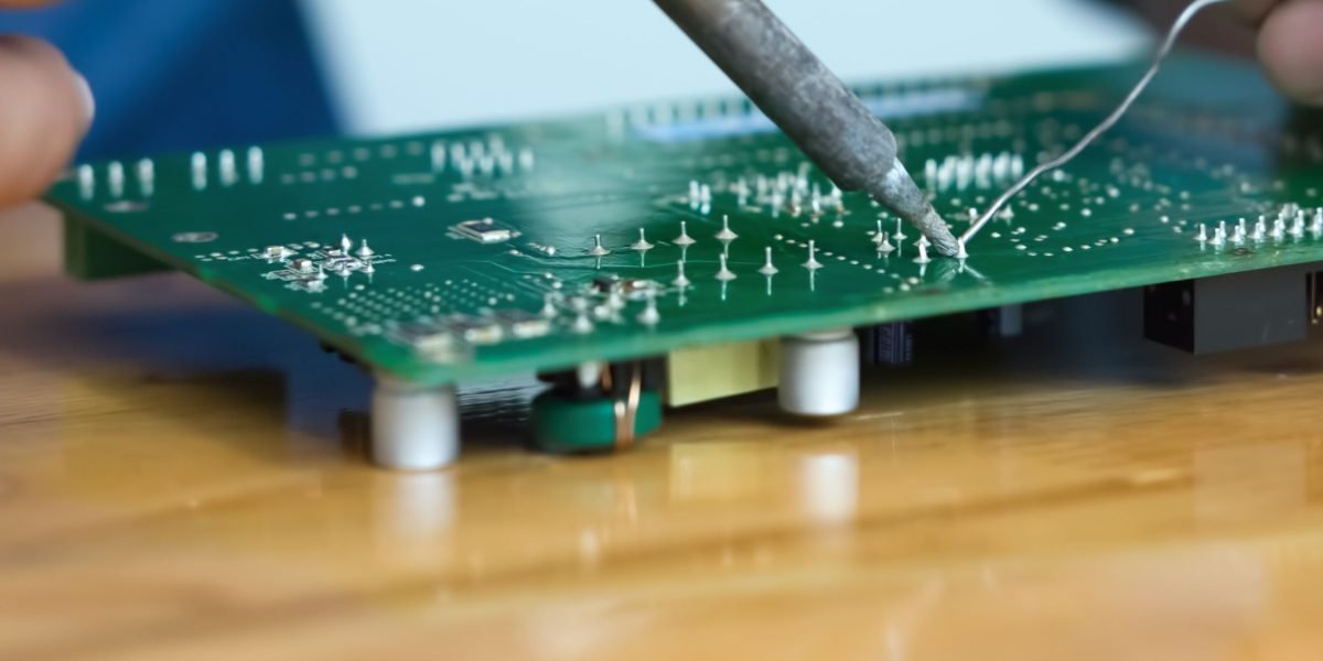
In today’s tech-driven world, nearly every electronic device we use—from smartphones to smart home gadgets—relies on a printed circuit board (PCB) at its core. But while many are familiar with the concept of PCBs, fewer understand the detailed process behind their assembly. The journey from a schematic design to a fully functional PCB is both intricate and fascinating.
In this blog, we’ll break down the PCB assembly process step-by-step, taking you through everything from initial design to final production.
What is PCB Assembly?
PCB Assembly (PCBA) refers to the process of soldering or mounting electronic components onto a bare printed circuit board to create a functioning electronic circuit. It’s important to distinguish between PCB (the board itself) and PCBA (the assembled board). The assembly process involves multiple stages, including solder paste application, component placement, soldering, and inspection.
Step 1: PCB Design and BOM Creation
Everything starts with a design.
a. Schematic Design
Before physical assembly can begin, engineers use software like Eagle, Altium Designer, or KiCAD to create a schematic diagram of the circuit. This schematic outlines how each component connects to others via copper traces.
b. PCB Layout
The schematic is translated into a PCB layout. This is where engineers define the physical placement of components on the board. Factors like board size, trace width, signal integrity, and thermal management are considered.
c. Bill of Materials (BOM)
The BOM is a comprehensive list of all the components required for assembly. It includes details like part numbers, quantities, reference designators (R1, C2, etc.), and manufacturers. A clear and accurate BOM is essential to avoid costly mistakes later.
Step 2: Sourcing Components
Once the design and BOM are finalized, the next step is component procurement. Manufacturers either purchase parts from authorized distributors or source them through supply chain partners.
Key considerations include:
- Availability: Are the components in stock?
- Lead time: How quickly can they be delivered?
- Authenticity: Are they genuine, quality-tested parts?
In some cases, customers may provide the components themselves—this is known as consigned assembly. Otherwise, the assembly house handles sourcing in what’s called turnkey assembly.
Step 3: Solder Paste Application
Solder paste is applied to the PCB in areas where components will be mounted. This is typically done using a stencil—a thin stainless steel sheet that masks off the board, allowing paste to be applied only where needed.
A solder paste printer applies the paste, which consists of tiny solder particles suspended in flux. Proper paste application is critical—too much or too little can cause poor solder joints or defects like bridging and tombstoning.
Step 4: Pick and Place
Once the paste is applied, it’s time to place the components.
A Pick and Place (PnP) machine picks components from reels or trays and places them precisely onto the solder-pasted areas of the PCB. These machines can put thousands of components per hour with incredible accuracy, down to fractions of a millimetre.
This step is mainly used for Surface Mount Technology (SMT) components, which are mounted directly onto the board’s surface.
Step 5: Reflow Soldering
After placement, the board passes through a reflow oven. This oven has multiple heating zones that gradually increase in temperature to melt the solder paste, forming permanent joints between components and the PCB.
The process includes:
- Preheat zone: Gradually heats the board to prevent thermal shock.
- Soak zone: Ensures even temperature distribution.
- Reflow zone: Reaches the melting point of the solder.
- Cooling zone: Solidifies the solder joints.
Reflow soldering is used primarily for SMT assembly. For Through-Hole Technology (THT) components, a different method—wave soldering or hand soldering—is used.
Step 6: Inspection and Quality Control
At this point, the board looks complete, but quality assurance is vital.
a. Automated Optical Inspection (AOI)
Cameras scan the PCB to detect soldering defects, missing components, misalignments, or short circuits.
b. X-Ray Inspection
Used for boards with Ball Grid Array (BGA) or hidden solder joints. X-ray helps verify internal connections that are invisible to optical methods.
c. Manual Inspection
Experienced technicians perform a visual check, especially for complex or high-value boards. Some defects are still best caught by human eyes.
Step 7: Functional Testing
Once the board passes visual inspection, it undergoes functional testing to ensure it works as intended. This may include:
- In-Circuit Testing (ICT): Checks individual components and connections.
- Flying Probe Testing: A less expensive, flexible alternative for small batches.
- Functional Testing (FCT): Verifies the board performs according to design specifications, often using test jigs and software.
This stage is crucial in catching issues before the product reaches the customer or is integrated into a larger system.
Step 8: Final Assembly and Packaging
For boards that are part of larger devices, additional steps might include:
- Installing connectors, heat sinks, or enclosures
- Programming microcontrollers
- Labelling or serializing each unit
After final assembly, boards are cleaned, packed in anti-static packaging, and prepared for shipping.
Challenges in PCB Assembly
While technology has made PCB assembly faster and more accurate, there are still challenges:
- Design flaws that aren’t caught early can derail production.
- Component shortages (like during global chip crises) can delay projects.
- Thermal stress during reflow can damage sensitive components.
- ESD (Electrostatic Discharge) can harm parts if proper precautions aren’t taken.
This is why working with an experienced and reliable PCB assembly partner is essential.
Conclusion
The PCB assembly process is a finely tuned combination of engineering, automation, and precision. From design and component sourcing to soldering and testing, every step plays a vital role in ensuring your product performs reliably in the real world.
Whether you’re a hardware startup or a seasoned manufacturer, understanding this process not only helps in planning and budgeting but also in making smarter design and production decisions.
As electronics continue to evolve, so too will PCB assembly—becoming faster, more sustainable, and even more advanced.
