Can the latest wearable devices maintain their sleek designs while packing more powerful features?
The demand for miniaturized, lightweight, and durable designs in wearable tech has led to the widespread adoption of flexible PCBs. These circuits are the backbone of modern wearable devices, enabling comfortable and feature-rich designs that conform to the human body.
As we push the boundaries of technology, we face significant challenges in designing and manufacturing PCBs that meet the requirements of wearable devices. For more insights on the future of PCB manufacturing, visit our article on the future of printed circuit board manufacturing.
Key Takeaways
- The role of flexible PCBs in enabling wearable device designs.
- Challenges in miniaturizing PCBs for wearable technology.
- The importance of balancing power and size in wearable devices.
- Trends in wearable device manufacturing and design.
- Future directions for PCB technology in wearables.
The Evolution of Wearable Technology PCBAs
The history of wearable technology is deeply intertwined with the progression of PCBA designs, from rigid to flexible solutions. As we explore this evolution, we gain insight into how wearable devices have become increasingly sophisticated.
From Rigid to Flexible: A Brief History
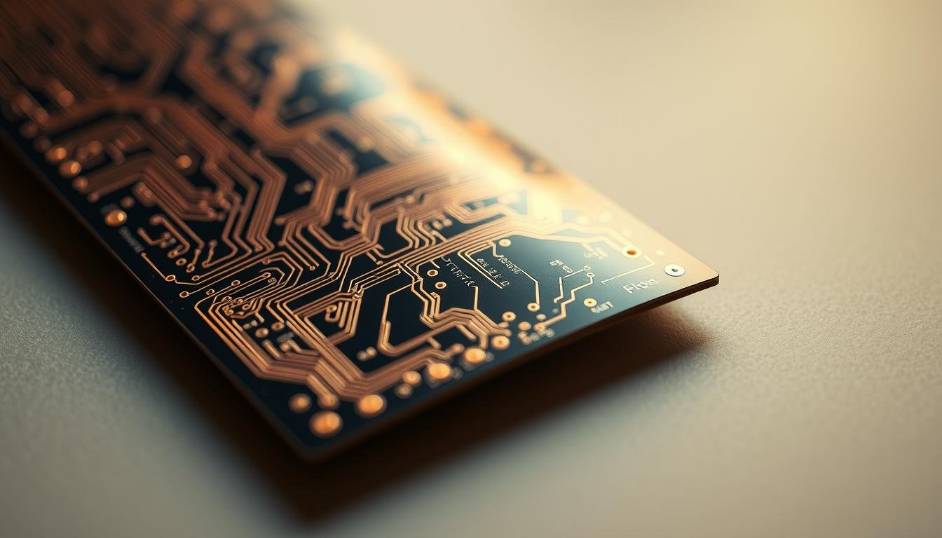
The transition from traditional rigid PCBs to flexible circuits represents a fundamental shift in how engineers approach wearable device design. Flexible PCBs, often called flex circuits, are thin, lightweight circuit boards made from flexible materials like polyimide. Unlike traditional rigid PCBs, they can bend, fold, and twist without breaking, making them perfect for compact and dynamic applications like wearable technology. This shift has enabled the development of more comfortable, lightweight, and feature-rich devices.
Why Miniaturization Matters in Wearable Devices
Miniaturization has become a driving force in wearable technology development, pushing manufacturers to pack more components and features into increasingly smaller spaces. The dramatic size reduction in wearable PCBAs has been enabled by key technological breakthroughs, maintaining or improving performance capabilities. As a result, modern wearables can offer a wide range of features without compromising on comfort or aesthetics.
| Feature | Rigid PCBs | Flexible PCBs |
|---|---|---|
| Design Flexibility | Limited | High |
| Space Efficiency | Low | High |
| Comfort | Limited by rigidity | Enhanced flexibility |
Understanding Flexible PCBs in Wearable Technology
As wearable technology continues to advance, the demand for more compact and efficient PCBs has become a critical challenge. Flexible PCBs are playing a crucial role in addressing this challenge by enabling the creation of smaller, more efficient wearable devices.
What Are Flexible PCBs?
Flexible PCBs, or flex-PCBs, are a type of printed circuit board that can bend and conform to various shapes, making them ideal for wearable technology applications. They are made from flexible materials, such as polyimide or polyester, which allow them to withstand repeated bending without compromising their functionality.
Advantages of Flex-PCBs for Wearable Devices
The use of flex-PCBs in wearable devices offers several advantages, including improved space efficiency, reduced weight, and enhanced reliability. Flex-PCBs can be designed to fit into compact spaces, making them perfect for applications where size is a constraint.
Common Applications in Smartwatches and Fitness Trackers
Flexible PCBs are widely used in smartwatches and fitness trackers due to their ability to conform to curved surfaces and withstand repeated bending. They enable the creation of sleek, compact designs that are both functional and comfortable to wear. Examples include the use of flex-PCBs in Apple Watch and Fitbit devices, where they play a crucial role in achieving the desired form factor and functionality.
Key Challenges of Miniaturization in Wearable Technology PCBA
Miniaturization in wearable technology PCBA presents several significant challenges. As wearable devices become increasingly compact, the design and manufacturing of their PCBs must adapt to these size constraints while maintaining functionality and reliability.
Space Constraints and Component Density
One of the primary challenges is managing space constraints and component density. Wearable devices require PCBs to be compact and densely packed with components, making it difficult to accommodate all necessary components, routing, and connections. This density can lead to increased complexity in PCB design.
- Densely packed components can cause thermal management issues.
- Compact designs often require innovative component placement strategies.
- Advanced PCB manufacturing techniques are necessary to achieve high component density.
Signal Integrity in Compact Designs
Another critical challenge is maintaining signal integrity in compact designs. As PCBs shrink, the risk of electromagnetic interference (EMI) and crosstalk between components increases. Ensuring signal integrity requires careful design and simulation.
Balancing Functionality with Size Limitations
Designers must strike a delicate balance between adding functionality and maintaining the small form factors demanded by consumers. This involves selecting components that are not only compact but also power-efficient and reliable.
“The key to successful miniaturization lies in innovative design and component selection.”
By understanding these challenges and leveraging advanced design and manufacturing techniques, we can create wearable devices that are both functional and compact.
Designing High-Density Interconnects for Wearable Devices
In the realm of wearable devices, HDI technology is pivotal in achieving the perfect balance between functionality and miniaturization. As wearable technology continues to evolve, the need for more complex yet compact PCBs has become increasingly important.
HDI Technology Fundamentals
HDI technology refers to a PCB design technique that significantly increases the number of connections per unit area. This allows for more functionality in a smaller footprint, making it especially crucial for devices like smartwatches and fitness trackers. By utilizing HDI, engineers can dramatically increase component density while maintaining reliable electrical connections in wearable PCBAs.
Microvias and Layer Stacking Techniques
Microvia technology is a key aspect of HDI, enabling the creation of multi-layer PCBs that fit within extremely limited spaces. These tiny connection points allow for complex circuitry in a compact form. Advanced layer stacking techniques further maximize functionality by utilizing the third dimension, rather than being confined to a traditional two-dimensional PCB plane.
Via-in-Pad Technology for Space Optimization
Via-in-pad technology is another critical space-saving approach in wearable PCBAs. By placing connection points directly under components, it eliminates the need for additional board real estate. This technique is vital in optimizing PCB design for wearable devices, where size is a significant constraint.
As stated by industry experts, “HDI technology is a game-changer in the wearable technology sector, enabling the production of smaller, more efficient devices.” The integration of HDI technology in wearable devices is a significant step forward in achieving the perfect balance between functionality and miniaturization.
Overcoming Flex-PCB Manufacturing Challenges
Flexible PCBs, crucial for modern wearable devices, demand innovative manufacturing solutions to address their inherent fragility and design complexities. Unlike rigid PCBs, flexible boards are more delicate and require specialized handling during manufacturing to avoid damage.
Material Selection for Durability and Flexibility
The choice of materials for flexible PCBs is critical, as it directly impacts their durability and flexibility. Manufacturers must select materials that can withstand the rigors of wearable device applications while maintaining their structural integrity. This involves a careful balance between material flexibility and the ability to support component density.
Managing Bend Radius and Stress Points
Proper management of the bend radius is essential to prevent stress-related failures at folding points in wearable devices. Engineers must design flexible PCBs with careful consideration of bend radius and stress points to ensure the longevity and reliability of the device. Techniques such as optimizing layer stacking and via placement can help mitigate these issues.
Assembly Considerations for Flexible Circuits
The assembly of flexible circuits requires specialized techniques and handling procedures that differ significantly from those used for rigid PCBs. This includes precise component mounting strategies and soldering approaches that minimize stress on the flexible PCB. By adopting these specialized assembly techniques, manufacturers can ensure the reliability and performance of wearable devices.
In conclusion, overcoming flex-PCB manufacturing challenges requires a comprehensive approach that addresses material selection, bend radius management, and assembly techniques. By understanding and addressing these challenges, we can improve the production of flexible PCBs for wearable technology.
Thermal Management Solutions for Compact Wearables
 is prominently displayed, its intricate design and components visible. Surrounding the ESPCBA, a network of heat sinks, heat pipes, and cooling fans work in harmony to efficiently dissipate the heat generated by the device's electronics. The middle ground features a translucent housing, allowing the viewer to observe the thermal management mechanisms in action. In the background, a minimalist, futuristic environment sets the stage, hinting at the advanced, space-saving nature of the wearable technology. Soft, diffused lighting illuminates the scene, emphasizing the sleek, modern aesthetic. The overall impression conveys the engineering challenges and innovative solutions required for effective thermal management in compact, flexible wearable devices.")
Compact wearables require innovative thermal management solutions to maintain performance and user comfort. As these devices shrink in size, managing heat dissipation becomes increasingly challenging.
Heat Dissipation in Miniaturized Designs
In densely packed wearable devices, excessive heat can degrade component performance and reduce battery life. Effective heat dissipation is crucial to maintaining the reliability and comfort of these devices.
Thermal Vias and Heat Spreaders
One effective method for managing heat in compact wearables is the use of thermal vias. These vias help dissipate heat from high-power components to the PCB’s inner layers or external heat sinks, distributing heat more evenly and preventing hot spots. Additionally, heat spreaders can be employed to further enhance thermal management.
Strategic Component Placement for Cooling
Strategic placement of components is another critical aspect of thermal management in wearables. By carefully positioning heat-generating components away from sensitive areas, we can significantly improve thermal performance without increasing the device’s size or weight.
| Thermal Management Technique | Description | Benefits |
|---|---|---|
| Thermal Vias | Dissipate heat from high-power components to PCB inner layers or external heat sinks | Even heat distribution, prevention of hot spots |
| Heat Spreaders | Enhance heat dissipation across the PCB | Improved thermal management, increased reliability |
| Strategic Component Placement | Position heat-generating components away from sensitive areas | Improved thermal performance, enhanced user comfort |
Power Efficiency Strategies for Wearable PCBAs
Power management in wearable PCBAs is crucial due to the limited battery size and the need for continuous operation. We must design PCBs that minimize power consumption while maintaining the device’s functionality and performance.
Low-Power Component Selection
Selecting components that consume minimal energy is vital. We look for low-power microcontrollers, sensors, and wireless communication modules with sleep modes and power-saving features. These components significantly reduce overall power consumption.
Power Management ICs and Circuit Design
Advanced power management ICs and circuit designs play a crucial role in extending battery life. We implement intelligent power distribution and sleep mode optimization to minimize power waste. This approach ensures that wearable devices operate efficiently.
Energy Harvesting Integration
Energy harvesting technologies offer a promising solution to supplement battery power in wearable devices. We explore kinetic, thermal, and solar energy harvesting methods integrated directly into the PCBA design. These technologies can significantly extend the operational life of wearable devices.
By implementing these strategies, we can significantly improve the power efficiency of wearable PCBAs, enhancing user experience through longer battery life and maintaining performance expectations.
Testing and Quality Assurance for Flex-PCBs
 undergoing rigorous testing procedures. The ESPCBA board is situated on a specialized testing rig, its intricate copper traces and solder joints illuminated by a combination of bright, diffused lighting and precision optics. Technicians in clean room attire carefully probe the board's connections, analyzing performance metrics and checking for any signs of stress or wear. The overall atmosphere conveys a sense of meticulous attention to detail and a commitment to ensuring the quality and reliability of these flexible, miniaturized electronics.")
The unique challenges faced by flexible PCBs in wearable applications necessitate specialized testing and quality assurance protocols. After assembly, flexible PCBs must be thoroughly tested to ensure they function under bending and flexing conditions. Specialized test fixtures simulate real-world usage, such as repeated wrist movements for a smartwatch, to verify durability and reliability.
Mechanical Stress Testing Protocols
Mechanical stress testing is critical to validate the performance of flexible PCBs under repeated bending and flexing. For instance, a flexible PCB might undergo 10,000 flex cycles during testing to confirm it won’t fail prematurely. This rigorous testing helps ensure that the PCB can withstand the mechanical stresses it will encounter during its lifespan.
Environmental Resilience Validation
Environmental testing approaches are also crucial to ensure that wearable PCBAs can withstand exposure to moisture, temperature fluctuations, UV light, and other real-world conditions. By simulating various environmental factors, manufacturers can predict and prevent potential failures, enhancing the overall reliability of the device.
Ensuring Long-Term Reliability
Reliability engineering principles are applied to flexible PCBs to predict their long-term performance in wearable applications. Accelerated life testing methods help identify potential failure points, allowing for design improvements and material selections that enhance durability. Comprehensive quality assurance programs contribute to reduced field failures and an enhanced brand reputation for wearable device manufacturers. As highlighted in a study on wearable technology advancements, thorough testing is pivotal for ensuring device reliability https://pmc.ncbi.nlm.nih.gov/articles/PMC11656044/.
Conclusion: Future Trends in Wearable Technology PCBA
The future of wearable technology is closely tied to advancements in PCBA design, particularly in miniaturization and flexibility. As wearable devices become more sophisticated, the demand for compact, efficient, and reliable PCBs is on the rise.
We’ve discussed the key challenges and solutions in miniaturizing PCBA for wearable applications, including the role of flexible PCBs and advanced manufacturing techniques. Emerging trends, such as the use of advanced materials like graphene and the integration of stretchable electronics, are poised to revolutionize wearable technology.
To stay competitive, manufacturers and engineers must prepare for these developments by adopting new materials and design techniques. By doing so, they can create wearable devices that not only track fitness and health metrics but also provide more complex functionalities, enhancing user experience and expanding the applications of wearable technology beyond fitness trackers and smartwatches.