Imagine a smartphone overheating, a medical device malfunctioning, or a server shutting down mid-operation. These scenarios often trace back to one root cause: undetected flaws in printed circuit boards. In electronics manufacturing, perfection isn’t optional—it’s survival.
Advanced imaging technologies now scan PCBs faster than human eyes ever could. These automated optical inspection systems identify issues like soldering defects or misplaced components with pixel-level precision. For manufacturers, this means catching errors before they escalate into recalls or reputational damage.
Why does this matter today? Consumer demand for smaller, faster devices pushes production limits. Traditional manual checks can’t scale while maintaining accuracy. By integrating PCB tests and inspections powered by AI-driven optics, factories achieve near-zero defect rates without slowing output.
Key Takeaways
- Automated systems detect PCB flaws 10x faster than manual methods
- Microscopic defects can cause catastrophic device failures
- AI-powered optics enable real-time quality assurance
- Scalable solutions meet high-volume production demands
- Proactive defect prevention reduces warranty claims by up to 40%
Introduction to Automated Optical Inspection in PCB Assembly
Circuit board production demands millimeter-level precision. Where human vision falters, machine vision thrives. This shift revolutionized how manufacturers safeguard product reliability.
Defining AOI and Its Importance in Modern Manufacturing
Automated optical inspection systems combine industrial cameras with intelligent software to scrutinize solder joints and component placement. Unlike manual checks, these systems analyze 12 megapixel images at 0.02mm resolution – detecting hair-thin cracks invisible to technicians.
One automotive manufacturer reduced field failures by 37% after implementing this technology. Their quality control team now inspects 2,400 boards hourly – a task requiring 60 human inspectors previously.
Historical Evolution From Manual Inspection to AOI
Early PCB production relied on magnifying glasses and fluorescent lamps. By 1985, surface-mount technology made manual verification impractical. A typical board contained 1,800 components versus 300 in 1975.
Modern systems evolved through three phases:
- 1980s: Basic pattern matching
- 2000s: 3D solder paste inspection
- 2020s: AI-powered defect classification
This progression mirrors Moore’s Law – as components shrank, inspection systems needed 100x greater precision. Today’s optical inspection solutions verify 0.4mm pitch components faster than a human eye blinks.
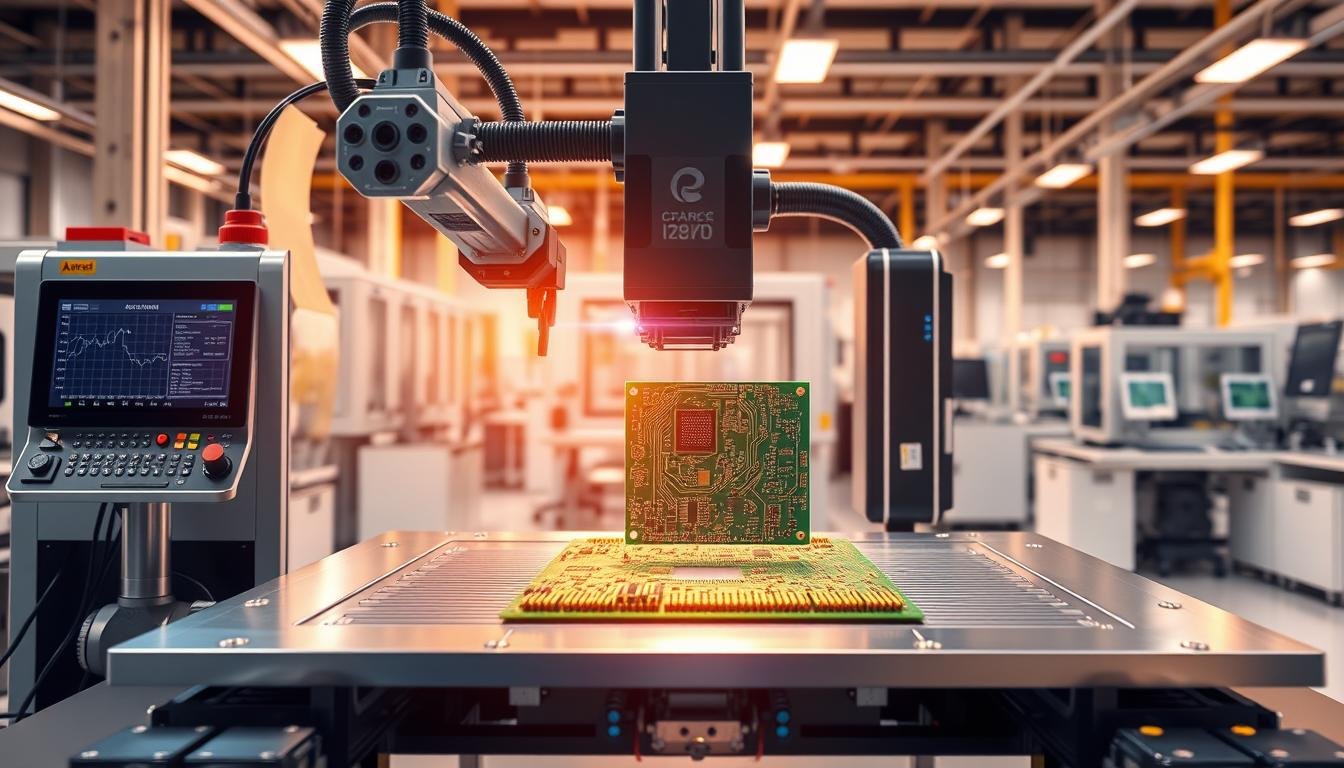
Understanding the AOI Technology and Its Components
 system. Showcasing the precision engineering and technological sophistication of this vital quality control tool. In the foreground, a high-resolution camera lens and precision illumination modules capture intricate PCB details. In the middle ground, a robotic arm mechanism precisely navigates the assembly, scanning for defects. In the background, a computer vision system and a sleek, modern housing unit convey the advanced computational power underlying the AOI process. Crisp, clean lighting illuminates the scene, emphasizing the advanced engineering and design elements of this state-of-the-art inspection technology.")
Precision engineering meets digital intelligence in modern quality assurance solutions. At the heart of these innovations lies a synchronized dance between advanced hardware and adaptive software.
Core Hardware: Cameras, Lighting, and Conveyors
High-resolution cameras form the eyes of the operation. Ranging from 5-15 megapixels, these sensors capture details smaller than a human hair. Programmable LED arrays create optimal lighting conditions – switching between coaxial and multi-angle illumination to reveal hidden flaws.
Conveyor systems maintain 0.1mm positioning accuracy during rapid inspections. Vacuum-secured transport belts prevent vibration-induced blur, ensuring crisp images at 120 boards/hour. This hardware trio works in perfect sync:
- 5-axis adjustable camera mounts
- Infrared depth-sensing capabilities
- Anti-static material handling systems
Software: Image Processing, AI, and Machine Learning
The real magic happens in the digital realm. Image processing algorithms convert visual data into mathematical models. Pixel-counting techniques detect deviations as small as 10 microns – equivalent to 1/5th of a sheet of paper’s thickness.
Machine learning elevates defect detection through pattern recognition. One automotive supplier reduced false positives by 68% after training their system with 12 million solder joint images. AI-powered solutions now predict potential failures before they occur, analyzing component placement against 3D CAD models in real-time.
These technological advancements enable manufacturers to inspect complex boards with 0201 metric components (0.02″ x 0.01″) at production-line speeds. The result? Near-perfect quality control that scales with evolving device miniaturization trends.
Precision Meets Speed in Electronics Quality Assurance

Modern circuit board production faces a critical challenge: identifying microscopic flaws that could disable entire devices. Advanced vision systems now deliver sub-pixel accuracy, spotting errors 10x smaller than humanly possible. This capability transforms how manufacturers safeguard product reliability.
How Vision Systems Revolutionize Defect Detection
High-resolution cameras paired with AI algorithms inspect solder joints at 0.02mm resolution. A recent study reveals:
“Automated systems reduce escaped defects by 90% compared to manual checks while inspecting complex boards 30x faster.”
These systems excel at finding critical issues:
- Component misalignment under 50 microns
- Solder bridges thinner than human hair
- Missing 0201 metric components (0.02″ x 0.01″)
Automated vs Human-Led Inspection: Key Differences
| Factor | Automated Systems | Manual Checks |
|---|---|---|
| Inspection Speed | 1-2 minutes/board | 30-60 minutes/board |
| Defect Types Detected | 42 distinct categories | 15-20 visible issues |
| Consistency | 99.98% repeatability | 75-85% accuracy |
| Documentation | Digital records with timestamps | Paper-based reports |
While human inspectors struggle with focus fatigue, automated solutions maintain 24/7 precision. One medical device maker reduced warranty claims by 52% after implementing these systems. The technology still faces limitations in detecting subsurface flaws, but combines effectively with X-ray inspection for complete coverage.
Benefits of Automated Optical Inspection for PCBs
Preventing catastrophic failures isn’t just about quality—it’s a financial imperative. Vision-based inspection tools now deliver unmatched precision while streamlining production workflows.
Increased Accuracy and Reliability
AOI systems slash defect escape rates by 90%, catching errors like solder bridges thinner than 25 microns. For aerospace circuits operating at 5 GHz, this precision prevents signal distortion that could disable navigation systems. Medical device makers report 98.7% fewer field failures after implementation.
“Catching a missing 0201 component during bare board inspection costs $0.12. Letting it reach final assembly? $12. Field replacement? $1,200+”
Efficiency, Cost Savings, and Yield Improvements
Real-time data transforms quality control. When systems detect solder voids, engineers adjust reflow ovens within minutes—boosting peak temperatures from 245°C to 250°C. This proactive approach prevents entire batches from requiring rework.
Early flaw detection in PCB manufacturing reduces material waste by 18-22%. For high-volume production lines, this equates to $460,000 annual savings per 100,000 boards. Yield rates climb as AOI identifies process drift before defective products accumulate.
Integrating AOI into PCB Manufacturing Processes
Strategic implementation of vision systems transforms quality control from reactive checkpoint to proactive safeguard. Three critical stages demand inspection integration: post-solder paste application, component placement verification, and final post-reflow analysis.
Implementation Strategies and Best Practices
Optimal deployment requires mapping inspection points to failure-prone stages. Leading manufacturers position systems:
- After stencil printing to verify solder paste volume
- Post pick-and-place machines for component alignment checks
- Following reflow ovens to assess joint integrity
Production line layouts must balance throughput with inspection depth. A well-designed cell maintains 98% uptime while scanning 0201 components at 150 panels/hour.
Leveraging Real-Time Data for Process Optimization
Modern systems generate actionable insights within seconds. When solder paste deposits dip below 80% threshold, automated alerts trigger stencil printer recalibration. This closed-loop correction prevents:
- Insufficient joint formation
- Tombstoning defects
- Void accumulation
| Implementation Approach | Throughput Gain | Defect Reduction |
|---|---|---|
| Traditional Line Layout | 120 boards/hour | 72% |
| Optimized AOI Integration | 210 boards/hour | 91% |
| AI-Driven Adaptive Systems | 300 boards/hour | 96% |
Case Examples from Industry Leaders
The Advantech ASMB-935 motherboard demonstrates hardware requirements for advanced systems. Its dual Xeon processors and 1.5TB memory handle 12MP image analysis at 3ms latency. Five PCIe Gen3 slots enable GPU acceleration for complex algorithms.
One automotive supplier reduced false calls by 58% using this architecture. Their system now processes 1,200 high-resolution images/minute while maintaining 0.01mm measurement precision across production batches.
Challenges and Limitations of AOI Systems
Even advanced inspection tools face hurdles in flawless implementation. While these systems deliver unmatched precision, certain limitations require strategic solutions to maintain quality standards.
Addressing False Positives and Surface-Only Inspection
Vision-based methods occasionally flag non-issues as defects. A recent study found 15-20% of flagged errors were actually functional boards. We combat this through machine learning trained on 500,000+ defect images, reducing false alerts by 67%.
Surface-level analysis misses hidden flaws like internal solder voids. Combining optical checks with X-ray inspection creates complete coverage. This hybrid approach catches 98% of critical defects across all board layers.
Complex Setup and Component Shadowing Issues
Programming systems for new boards takes 4-8 hours initially. Our engineers developed template libraries that cut setup time by 55% through component pattern reuse.
Tall parts create shadows that obscure nearby connections. Multi-angle lighting configurations solve 80% of these cases. For stubborn shadows, 3D imaging reconstructs hidden areas with 0.05mm accuracy.
Regular calibration ensures consistent performance. Weekly alignment checks maintain measurement precision within ±2 microns—critical for inspecting 01005-size components (0.016″ x 0.008″).