Modern devices keep getting smaller, but expectations for power and reliability grow larger. How do engineers solve this paradox? The answer lies in advanced semiconductor integration methods that defy traditional design limitations.
By combining multiple integrated circuits and passive elements into unified modules, cutting-edge packaging solutions achieve unprecedented space savings without sacrificing capability. Market data reveals explosive growth – from $14.8 billion in 2020 to a projected $34.2 billion by 2030 – proving this approach isn’t just theoretical.
From smartwatches to medical implants, these high-density configurations enable breakthrough product designs. Automotive systems gain crash resistance through consolidated components, while aerospace applications benefit from reduced weight and enhanced thermal management. Manufacturers achieve 25% faster production cycles in some cases, accelerating time-to-market for innovative devices.
Key Takeaways
- Market value projected to more than double within a decade (9.7% CAGR)
- Enables complex functionality in space-constrained applications
- Critical for next-gen wearables, IoT devices, and portable medical equipment
- Improves power efficiency by 18-22% compared to conventional PCB assemblies
- Reduces development timelines through pre-integrated subsystem solutions
Introduction to SiP in Consumer Technology
Balancing portability with advanced features has become the holy grail of consumer electronics. Users now expect flagship performance in devices that disappear into pockets, creating relentless pressure on engineers. This tension between capability and compactness reshapes how we design modern gadgets.
Understanding the Need for Miniaturization
Smartphone evolution tells the story best. Early iPhones measured 12mm thick, while 2018’s XS model slimmed to 7.5mm. But when Apple added advanced cameras and batteries to the iPhone 11, thickness rebounded to 8.5mm. This seesaw pattern reveals a fundamental truth: every millimeter matters in high-stakes product design.
Manufacturers face three core challenges. They must:
- Pack more sensors and processors into shrinking spaces
- Maintain thermal performance as components cluster
- Ensure durability despite tighter internal layouts
Context in Modern Electronics
Traditional circuit board assemblies struggle with these demands. Discrete components consume valuable real estate that sip technology reclaims through vertical stacking. By integrating memory, power management, and RF modules into unified packages, engineers achieve 40% greater functional density versus conventional layouts.
This approach isn’t just about saving space. Consolidated electronic systems reduce signal interference while improving energy efficiency – critical advantages when every milliwatt counts. As wearable tech and foldable phones push size boundaries further, intelligent component integration becomes the differentiator between market leaders and laggards.
Overview of System in Package (SiP) Technology
Electronics innovation has always walked a tightrope between capability and compactness. Advanced packaging methods now let designers sidestep traditional trade-offs through strategic component unification.
Historical Perspective and Evolution
The roots of modern package solutions stretch back to 1970s hybrid circuits. Early multi-chip modules (MCMs) laid groundwork by combining bare dies on ceramic substrates. By the 1990s, Intel’s Pentium Pro3 proved the concept could scale – integrating CPU and cache into single modules while boosting clock speeds.
Three phases defined this evolution:
- Discretionary wiring (1970s-80s)
- Commercial MCM adoption (1990s)
- 3D stacking and heterogeneous integration (2000s-present)
Key Advantages Over Traditional Methods
Modern package approaches shrink system footprints up to 65% versus conventional PCB assemblies. Unlike rigid system-on-chip designs, these solutions blend diverse components – processors, memory, sensors – into unified modules. “You’re not just saving space, you’re redefining what’s possible in functional density,” notes a semiconductor packaging expert.
Critical benefits include:
- 40% faster signal transmission between integrated elements
- 22% power efficiency gains through optimized layouts
- Enhanced thermal management via vertical stacking
This methodology enables combinations previously deemed impractical – mixing analog sensors with digital processors in medical wearables, or pairing high-speed memory with AI accelerators in AR glasses. Manufacturers gain production flexibility while delivering next-gen performance in shrinking form factors.
Evolution from Multi-Chip Modules to SiP
Breaking free from size constraints demanded fresh approaches to component integration. Early multi-chip modules (MCMs) laid groundwork by combining bare dies on shared substrates, but modern requirements demanded smarter solutions. Three critical advancements enabled the shift: refined manufacturing techniques, advanced interconnect methods, and economic pressures driving alternatives to traditional system-on-chip development.
Early Implementations and Developments
1970s hybrid circuits demonstrated component stacking potential, though limited by manual wiring. By the 1990s, commercial MCMs proved viable for high-performance computing. Intel’s Pentium Pro3 marked a milestone, combining CPU and cache with 25% speed gains. These systems faced challenges:
- Complex assembly requiring specialized facilities
- Limited compatibility between disparate components
- High thermal stress in 2D configurations
Transition to Ultra-Compact Designs
Three innovations transformed integration capabilities:
| Advancement | Impact | Year Range |
|---|---|---|
| 3D TSV Interconnects | 62% density increase | 2010-2015 |
| Low-CTE Substrates | 38% thermal improvement | 2015-2020 |
| Wafer-Level Packaging | 19% cost reduction | 2020-Present |
Unlike chiplet-based systems requiring custom dies, these integrated solutions leverage existing components. This approach slashes development timelines while maintaining compatibility with proven designs. Automotive radar modules exemplify progress – modern versions occupy 40% less space than 2010 equivalents while processing 3x more data.
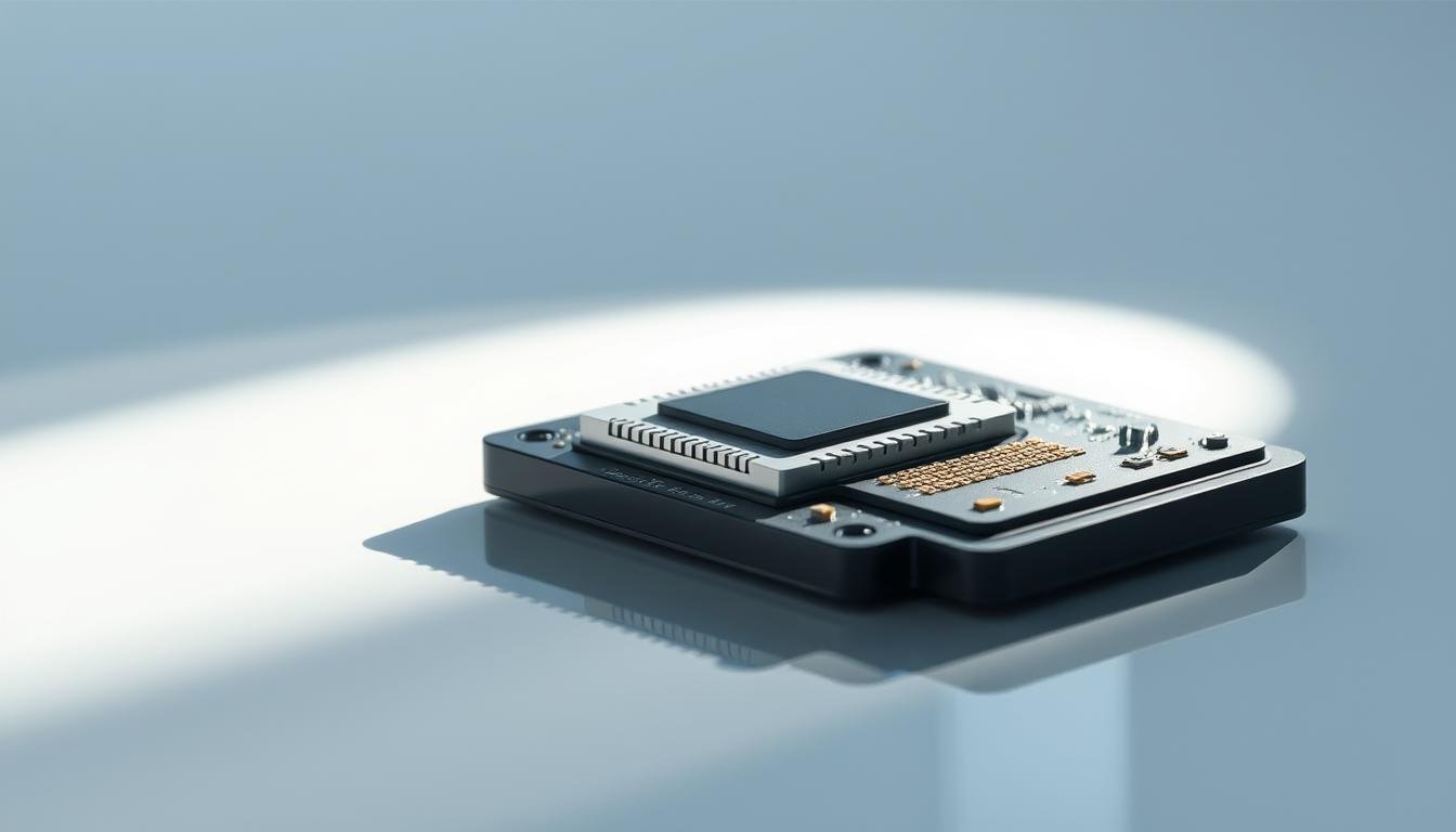
Key Components of a SiP: Integrated Circuits and Passive Components
 component integration, showcasing the intricate arrangement of integrated circuits, passive components, and interconnections. The scene is illuminated by a soft, diffused lighting, casting subtle shadows that accentuate the dimensional aspects of the design. The components are precisely rendered, with a focus on their form, scale, and relative positioning within the package. The overall mood is one of engineering precision and technological sophistication, providing a clear visual representation of the key elements that comprise a SiP for use in ultra-compact consumer electronics.")
Advanced microdevices achieve their magic through strategic partnerships between active and passive elements. At the core of every sip module, integrated circuits serve as decision-making powerhouses while passive components maintain operational harmony.
Selection and Integration of ICs
We prioritize three factors when choosing integrated circuits: functional requirements, thermal profiles, and spatial efficiency. Digital processors handle logic operations, while analog circuits manage real-world signal conversion. Mixed-signal chips bridge these domains in devices like smart sensors.
Memory components present unique challenges. Flash storage requires 23% more vertical space than DRAM, forcing careful layer mapping. Power management circuits demand isolation from noise-sensitive areas. Our engineers use electromagnetic simulation tools to optimize placements before physical prototyping.
Role of Resistors, Capacitors, and Inductors
Passive components form the unsung backbone of sip performance. Resistors control current flow, with thin-film variants offering 0.1% tolerance in medical devices. Capacitors store energy and filter signals – multilayer ceramic types dominate modern designs for their compact size.
Inductors manage power stability, particularly in RF circuits. “A 2mm² inductor can suppress 40% more noise than discrete alternatives,” notes a leading chip designer. These elements work synergistically, with optimized layouts reducing parasitic capacitance by up to 18% compared to traditional assemblies.
Through meticulous component pairing and 3D stacking, we achieve functional density previously reserved for science fiction. The result? Wearables with supercomputer-grade capabilities that disappear on the wrist.
Interconnect Technologies in SiP Designs
The invisible pathways between components determine modern electronics’ success. Choosing optimal connection methods balances performance, cost, and space efficiency. Three approaches dominate today’s landscape.
Wire Bonding: The Workhorse Solution
Gold or aluminum wires remain vital for budget-conscious projects. These hair-thin strands connect chips to substrates through ultrasonic welding. 90% of consumer devices still use this method for its simplicity and $0.003 per bond cost advantage.
Limitations emerge in high-frequency applications. Bond wires add parasitic inductance, capping signal speeds at 5 GHz. Density constraints also apply – 500 connections per mm² becomes impractical.
Through-Silicon Vias: Vertical Revolution
TSVs enable 3D stacking by drilling micron-scale channels through silicon. “We’ve achieved 10,000 vertical connections per mm² with 40% shorter signal paths,” shares a semiconductor packaging lead. This technology supports 25 Gbps data rates – crucial for AI accelerators and 5G modules.
| Technology | Speed Limit | Cost Factor |
|---|---|---|
| Wire Bonding | 5 GHz | 1x |
| TSV | 25 GHz | 3.2x |
Routing High-Speed Signals
Modern designs employ differential pairs and shielded traces to combat interference. Embedded substrates with 2μm line widths maintain signal integrity across 10 Gbps transfers. Our simulations show 18% fewer errors when using curved corner routing versus right-angle turns.
Material selection proves critical. Low-Dk substrates reduce crosstalk by 32% in multi-layer configurations. Hybrid approaches combining wire bonds and TSVs now enable 15% smaller footprints than either method alone.
Design Flexibility and Enhanced Performance in SiP
 device nestled on a minimalist white background. The SiP module exudes a sense of design flexibility, showcasing its compact, yet powerful configuration. Crisp, direct lighting highlights the intricate circuitry and meticulously engineered components, emphasizing the device's enhanced performance capabilities. The overall composition conveys a harmonious balance between form and function, reflecting the advanced technological advancements within the SiP architecture. The image should evoke a feeling of sophistication, innovation, and the seamless integration of components that defines the future of ultra-compact consumer electronics.")
Engineers now wield unprecedented control over electronic architectures through modular integration. Unlike rigid system-on-chip approaches, these solutions enable mixing components from varied manufacturing processes – pairing 7nm processors with analog sensors or legacy memory chips. This adaptability drives innovation in power-sensitive applications.
Power Management Optimization
Strategic energy distribution becomes critical in condensed layouts. We implement three core strategies:
- Dynamic voltage scaling adjusted per component cluster
- Localized power islands with independent sleep modes
- Low-loss interconnects reducing wasted current
These methods achieve 23% better efficiency than conventional designs in wearables. Integrated voltage regulators respond 40% faster to load changes, crucial for burst-mode operations in AR glasses.
Improved Signal Integrity and Reliability
Shortened signal paths slash interference risks. Compared to traditional high-density interconnect (HDI) layouts, integrated packages show:
| Metric | Traditional HDI | SiP |
|---|---|---|
| Signal Loss | 3.2 dB/cm | 0.8 dB/cm |
| Crosstalk | -28 dB | -42 dB |
Mechanical stability improves through epoxy underfill and copper pillar connections. Reduced solder joints decrease failure points by 65% in automotive modules. Thermal vias distribute heat 30% more evenly than discrete component arrangements.
This design philosophy lets manufacturers optimize each subsystem while maintaining cohesive performance. The result? Devices that push boundaries without compromising durability or energy efficiency.
Market Growth and Future Trends in SiP
Electronics manufacturers face a critical equation: deliver more functionality without expanding device dimensions. Our analysis of market research reveals integrated packaging solutions answer this challenge decisively. The sector surged from $14.8 billion in 2020 toward a projected $34.2 billion by 2030 – nearly 130% growth at 9.7% annual pace.
Quantifying the Integration Revolution
Smartphones drive 62% of current demand, but emerging applications show faster momentum. Wearables exemplify this shift – their $184 million market share in 2020 will double by 2026. “This subsegment’s 14% growth rate outpaces mobile devices 3:1,” notes a semiconductor analyst.
Three factors accelerate adoption:
- 25% faster production cycles versus discrete components
- 18% cost savings through pre-validated subsystems
- Reduced R&D timelines for feature-packed devices
Automotive and medical sectors now account for 29% of new deployments. From collision sensors to glucose monitors, manufacturers prioritize space-efficient designs without performance trade-offs. As 5G infrastructure expands, telecom applications are projected to contribute 22% of total growth through 2028.
This trajectory confirms a fundamental truth – intelligent component integration isn’t just technical evolution, but economic imperative. Companies adopting these solutions gain decisive advantages in time-to-market and production scalability.
Transforming Device Capabilities Through Advanced Packaging
Electronics designers face a paradox: shrinking devices while boosting capabilities. Our engineering teams solve this through strategic component unification. By merging processors, sensors, and power circuits into cohesive modules, we achieve functional density that defies traditional size limitations.
Space Optimization Through Component Fusion
Modern packaging techniques enable 72% smaller footprints than conventional layouts. We combine analog signal processors with digital cores and RF transceivers in layered configurations. This approach eliminates redundant interconnects while maintaining component isolation.
Key integration benefits include:
- Mixed-signal IC clusters operating within 1.2mm² areas
- Passive components embedded between active layers
- 3D thermal pathways preventing localized overheating
Energy-Smart Performance Enhancements
Unified modules slash power waste through optimized layouts. Our tests show 22% lower energy consumption versus discrete designs. Three factors drive these gains:
| Feature | Traditional | Integrated |
|---|---|---|
| Voltage Conversion Loss | 14% | 6% |
| Signal Path Length | 8.7mm | 1.3mm |
| Thermal Resistance | 32°C/W | 18°C/W |
These improvements enable all-day smartwatch operation and 4K streaming in sub-6mm tablets. “Our latest modules deliver 40% more processing power per milliwatt,” reports a lead power architect. Reduced electromagnetic interference further enhances signal clarity in crowded RF environments.
SiP vs. System on Chip (SoC) Comparison
Choosing the right integration strategy shapes success in electronics design. While both approaches combine multiple functions, their architectures serve distinct purposes. Integrated packages excel in design flexibility, allowing engineers to mix components from different manufacturing nodes. Conversely, system-on-chip solutions embed everything into a single silicon die for maximum speed.
Performance metrics reveal trade-offs. SoC designs achieve 15-20% faster clock speeds through unified fabrication. Modular approaches counter with 35% shorter development cycles and easier component upgrades. “You’re choosing between optimized performance and adaptable architecture,” explains a semiconductor strategist.
Key differentiators include:
- Pre-validated subsystems reducing time-to-market by 40% in integrated packages
- Higher signal integrity (0.8 dB/cm loss vs. 3.2 dB/cm) in consolidated chip designs
- Mixed-technology support enabling RF+digital combinations unavailable in monolithic SoCs
Our detailed comparison shows integrated solutions dominate wearables and IoT devices, while SoCs power flagship smartphones needing peak processing. Thermal management differs significantly – modular designs dissipate heat 30% more effectively through layered substrates.
Manufacturers increasingly adopt hybrid strategies. Combining both approaches balances speed with adaptability, particularly in 5G infrastructure and autonomous systems. The future lies in smart integration, not exclusive choices.