As electronic devices become increasingly compact and modular, the role of castellated holes in PCB design has gained significant importance. These specialized structures enable engineers to connect PCBs directly, simplifying assembly and enhancing overall system efficiency.
But what makes castellated holes so crucial in modern PCB manufacturing? We explore how these plated half-holes are revolutionizing the way we design and manufacture printed circuit boards, enabling more compact, durable, and efficient electronic systems.
Key Takeaways
- Understanding the role of castellated holes in modern PCB design
- The benefits of using castellated holes in PCB manufacturing
- How castellated holes enhance connectivity, durability, and space efficiency
- The importance of design considerations for castellated holes
- Practical applications of castellated holes in cutting-edge electronics
Understanding Castellated Holes in PCB Design
As PCB design continues to evolve, the importance of castellated holes in achieving seamless board-to-board connections cannot be overstated. We will delve into the intricacies of these features, exploring their definition, structure, and significance in modern electronics.
Definition and Structure of Castellated Holes
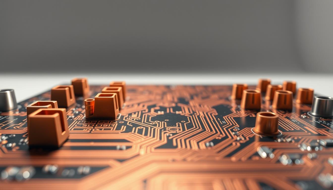
Castellated holes are half-circular, plated indentations located along the edges of a PCB, designed to facilitate direct board-to-board connections. Unlike standard vias or plated-through holes (PTH), which connect layers within a board, castellated holes are created by drilling full holes during fabrication and then milling them in half, leaving a plated semi-circle exposed on the board’s edge. This process ensures a reliable electrical and mechanical connection when soldered to another PCB or component.
- Enable direct board-to-board connections
- Created through a process of drilling and milling
- Feature plated semi-circles for reliable connections
Historical Development and Modern Applications
The concept of castellated holes has evolved significantly since its inception, driven by advancements in PCB manufacturing techniques. Initially, these features were rudimentary and limited in their application. However, as technology progressed, castellated holes became more refined, precise, and adaptable to complex designs. Today, they are a cornerstone of surface-mount technology (SMT), enabling seamless integration in space-constrained applications.
Castellated holes have become particularly valuable in applications where space efficiency is crucial, such as in wireless communication modules, IoT devices, and wearable technology. Their ability to facilitate compact, reliable connections has made them an indispensable feature in modern PCB design.
The Manufacturing Process of Castellated Holes
The creation of castellated holes in PCB design involves a multi-step manufacturing process that requires precision and expertise. We will delve into the intricacies of this process, highlighting the critical stages and techniques involved.
Drilling and Milling Techniques
The manufacturing process begins with drilling full holes through the PCB substrate. This step requires specialized drilling parameters, including adjusted speed, pressure, and bit type, to ensure accuracy and prevent damage to the board. Following drilling, the board is profiled, and a part of the hole is cut off during the milling process, creating the characteristic castellated edge.
Advanced CNC milling techniques are employed to achieve the desired precision, with some machines operating at speeds up to 50,000 RPM. This high-speed milling, combined with post-process deburring, helps eliminate common manufacturing defects.
Plating Methods and Materials
After milling, the exposed half-holes are plated with conductive materials like copper or gold to ensure good electrical conductivity. The plating process involves a separate chemical process, requiring its own set of tools and safety measures.
| Plating Material | Electrical Conductivity | Mechanical Properties |
|---|---|---|
| Copper | High | Ductile |
| Gold | High | Corrosion-resistant |
Post-plating inspection is essential to ensure that the coating is uniform and meets the specified requirements. By employing precision manufacturing equipment and processes, we can create reliable castellated holes that meet IPC standards.
Key Advantages of Using Castellated Holes

We explore the key advantages of castellated holes, a crucial element in modern PCB design. Castellated holes bring several benefits, making them a go-to solution for engineers. The plated edges provide a strong electrical link between boards, reducing signal loss.
Enhanced Electrical Connectivity
Castellated holes offer enhanced electrical connectivity by providing a direct, plated connection between PCBs. This is particularly important in high-frequency applications, such as RF modules operating at 2.4 GHz, where maintaining signal integrity is critical. By minimizing signal loss and interference, castellated connections result in improved circuit performance.
Space Efficiency and Compact Design
The use of castellated holes enables space efficiency and compact design by eliminating the need for bulky connectors. This is especially beneficial for miniaturized electronics, such as wearable devices. For instance, a 20mm x 20mm wearable device can stack multiple boards using castellated holes, significantly reducing the overall size.
Improved Mechanical Durability
Castellated connections also offer improved mechanical durability compared to traditional connectors. They withstand repeated assembly and disassembly cycles, making them suitable for modular systems like IoT devices. This durability, combined with simplified assembly and reduced manufacturing costs, makes castellated holes an optimal solution for high-volume production.
What is Castellated Holes in PCB Design: Practical Applications

Castellated holes have become a crucial component in modern electronics, enabling seamless connections between various PCB components. We will explore the diverse practical applications where castellated holes have become the preferred connection method in modern electronics.
Wireless Communication Modules
Devices like Wi-Fi, Bluetooth, and RF modules rely heavily on castellated holes for easy integration with mainboards. For instance, a Bluetooth Low Energy (BLE) module might use castellated holes to connect to a mainboard, ensuring a reliable link at 2.4 GHz. This application highlights the importance of castellated holes in maintaining signal integrity and facilitating compact designs.
IoT Devices and Wearable Technology
The modular nature of IoT systems, such as smart sensors or connected wearables, makes castellated holes ideal for linking components like processors, antennas, and power modules. Compact gadgets, such as fitness trackers or smartwatches, leverage castellated holes to maintain small form factors while ensuring robust connections. For more information on the advantages and applications of castellated holes, visit this comprehensive guide.
Breakout Boards and Prototyping
Breakout boards, popular in prototyping, use castellated holes to mount onto larger systems. A microcontroller breakout board, for example, can be soldered directly to a development board for testing, simplifying the prototyping process. The use of castellated holes in breakout boards eliminates the need for additional connectors, streamlining the development process.
| Application | Benefits of Castellated Holes |
|---|---|
| Wireless Communication Modules | Reliable signal transmission, compact design |
| IoT Devices and Wearable Technology | Modular design, robust connections, small form factor |
| Breakout Boards and Prototyping | Simplified prototyping, reduced need for additional connectors |
Essential Design Considerations for Castellated Holes
To successfully incorporate castellated holes into your PCB design, it’s crucial to understand the essential design considerations. Castellated holes require precise design to meet both manufacturing and functionality requirements.
Optimal Hole Size and Spacing Parameters
The minimum diameter for castellated holes is typically 0.5mm, with a spacing of at least 0.5mm between holes. While smaller sizes (e.g., 0.3mm) are possible, they demand advanced fabrication tools, increasing manufacturing costs. Careful consideration of hole size and spacing is vital for manufacturability and performance.
Surface Finish Selection
Electroless Nickel Immersion Gold (ENIG) is a popular surface finish choice due to its corrosion resistance and solderability. For high-reliability applications, a gold thickness of 0.05-0.1µm over 3-6µm of nickel ensures long-term performance. The right surface finish can significantly impact the reliability and durability of castellated holes.
Pad Design and Placement Guidelines
Larger pads improve solder joint strength. Aim for an annular ring of at least 0.25mm on both the top and bottom layers. For a 0.5mm hole, a 1mm pad diameter is a solid starting point. Additionally, keep castellated holes away from components and traces to avoid interference during soldering, maintaining a clearance of at least 0.5mm from nearby features.
By carefully considering these design factors, you can ensure the successful implementation of castellated holes in your PCB projects, balancing manufacturability with performance.
Overcoming Manufacturing Challenges
Producing high-quality castellated holes demands overcoming manufacturing challenges such as precision alignment and plating integrity. The process of creating these holes is complex and requires careful attention to detail to ensure the final product meets the required standards.
Addressing Copper Burrs and Plating Integrity
Milling the half-holes can leave copper burrs inside, risking weak solder joints or shorts. We utilize advanced CNC milling with speeds up to 50,000 RPM and post-process deburring to eliminate this issue. The plating must remain intact after milling; poor plating can lead to connection failures. To counter this, we employ precise electroplating and quality checks, ensuring thickness meets IPC Class 3 standards (25-35µm).
Key Considerations for Copper Burrs and Plating:
- Copper burr removal through deburring
- Maintaining plating integrity with precise electroplating
- Ensuring plating thickness meets IPC Class 3 standards
Ensuring Precision Alignment and Quality Control
Misaligned holes disrupt board-to-board soldering. Tolerances as tight as ±0.05mm are achievable with modern laser-guided milling machines, ensuring perfect fitment. We implement rigorous quality control measures to guarantee accurate placement and consistent results.
| Manufacturing Aspect | Challenge | Solution |
|---|---|---|
| Copper Burrs | Risk of weak solder joints or shorts | Advanced CNC milling and deburring |
| Plating Integrity | Poor plating leading to connection failures | Precise electroplating and quality checks |
| Precision Alignment | Misaligned holes disrupting soldering | Laser-guided milling machines |
By addressing these manufacturing challenges, we ensure the production of high-quality castellated holes that meet the stringent requirements of modern PCB assembly.
Conclusion
By integrating castellated holes into PCB design, engineers can achieve superior electrical connectivity and mechanical durability. Castellated holes have become a crucial component in modern electronics manufacturing, offering a unique blend of compactness and functionality.
The key benefits of castellated holes include enhanced electrical connectivity, space efficiency, and improved mechanical durability. These advantages make them an ideal solution for various applications, from wireless communication modules to IoT devices and prototyping solutions.
To ensure successful implementation, it’s essential to follow proper design guidelines, including optimal hole sizing, surface finish selection, and pad design. While manufacturing challenges exist, they can be overcome with the right expertise and quality control processes.
We recommend that engineers considering castellated holes for their next project balance design requirements with manufacturing capabilities. By doing so, they can unlock the full potential of this technology and create innovative, compact electronic systems. To get started, leverage our expertise in PCB manufacturing to bring your castellated hole designs to life with precision and reliability.