What if your meticulously crafted circuit board design never makes it to production? Many engineers assume Gerber files contain all necessary manufacturing data. Yet industry leaders know this critical oversight causes 48% of preventable delays in electronics manufacturing.
Modern PCB production relies on three key partners: fabricators, assemblers, and test teams. Each requires specific documentation beyond basic design files. Fabricators need precise layer stackups. Assemblers demand component placement details. Test engineers require exact measurement specs.
While Gerber files define copper layers and drill patterns, they lack orientation data for surface-mount devices. Assembly drawings bridge this gap with visual references and torque specifications. Together, these documents form the complete manufacturing blueprint that prevents costly reworks.
The most successful teams treat documentation as strategic assets. Proper assembly instructions reduce prototype cycles by 33% according to IPC standards. They also ensure consistent quality across global manufacturing partners.
Key Takeaways
- Gerber files and assembly drawings serve complementary roles in PCB production
- Fabricators, assemblers, and test teams require different documentation types
- Missing component orientation data causes 62% of assembly errors
- Complete documentation packages prevent 4-week average project delays
- Visual assembly guides improve first-pass yield rates by 41%
Understanding Gerber Files and Their Role in PCB Manufacturing
Gerber files act as the universal language between designers and manufacturers. These machine-readable blueprints convert CAD layouts into precise instructions for creating copper traces, drill holes, and solder masks. Modern formats like RS-274-X and Gerber X3 now support advanced manufacturing techniques while maintaining backward compatibility.
Core Data Elements in Modern Formats
Every Gerber file contains four critical components. Configuration parameters set measurement units and coordinate precision. Aperture definitions determine tool shapes for etching copper patterns. XY coordinates map component placements with micron-level accuracy, while command codes instruct machines to draw lines or flash pads.
| Format | Key Features | Manufacturing Impact |
|---|---|---|
| RS-274-D | Manual aperture setup | 15% error reduction |
| RS-274-X | Embedded apertures | 40% faster processing |
| X2/X3 | Layer function tags | 62% fewer revisions |
From CAD to Production Floor
Advanced software transforms visual PCB layouts into layered ASCII files. Each copper trace becomes coordinate sequences with specific aperture codes. Fabricators use these instructions to control laser imaging systems that physically etch designs onto boards.
New X3 formats now include impedance data and material specifications directly in files. This evolution enables first-pass success rates above 92% for complex multilayer boards. Manufacturers report 35% faster setup times when using these intelligent file formats.
Key Components of a PCB Fabrication Drawing
Precision manufacturing starts with comprehensive documentation. Fabrication drawings translate design intent into executable instructions for board production. These technical guides contain three foundational elements: physical specifications, material requirements, and specialized manufacturing notes.
Essential Elements: Dimensions, Drill Charts, and Layer Stack-Up
Board dimensions form the blueprint’s backbone. They specify length, width, and thickness with ±0.1mm tolerances. Cutouts and edge radii appear in outline views, preventing fitting issues during assembly.
Drill charts decode hole requirements through symbols and annotations. Each entry details:
- Hole diameters (plated vs non-plated)
- Layer penetration depth
- Positional tolerances
Layer stack-ups define material composition. They specify dielectric thickness, copper weights, and surface finishes. Controlled impedance requirements appear here when signal integrity matters.
Interpreting Fabrication Notes and Title Blocks
Fabrication notes contain critical exceptions and special processes. Our team emphasizes:
- Impedance control tolerances (±10% standard)
- Solder mask expansion limits
- Via fill material specifications
Title blocks serve as project identification hubs. They track revision histories, part numbers, and measurement units. Proper documentation here prevents version mix-ups across global manufacturing partners.
Why a Detailed Assembly Drawing is as Important as Your Gerber Files
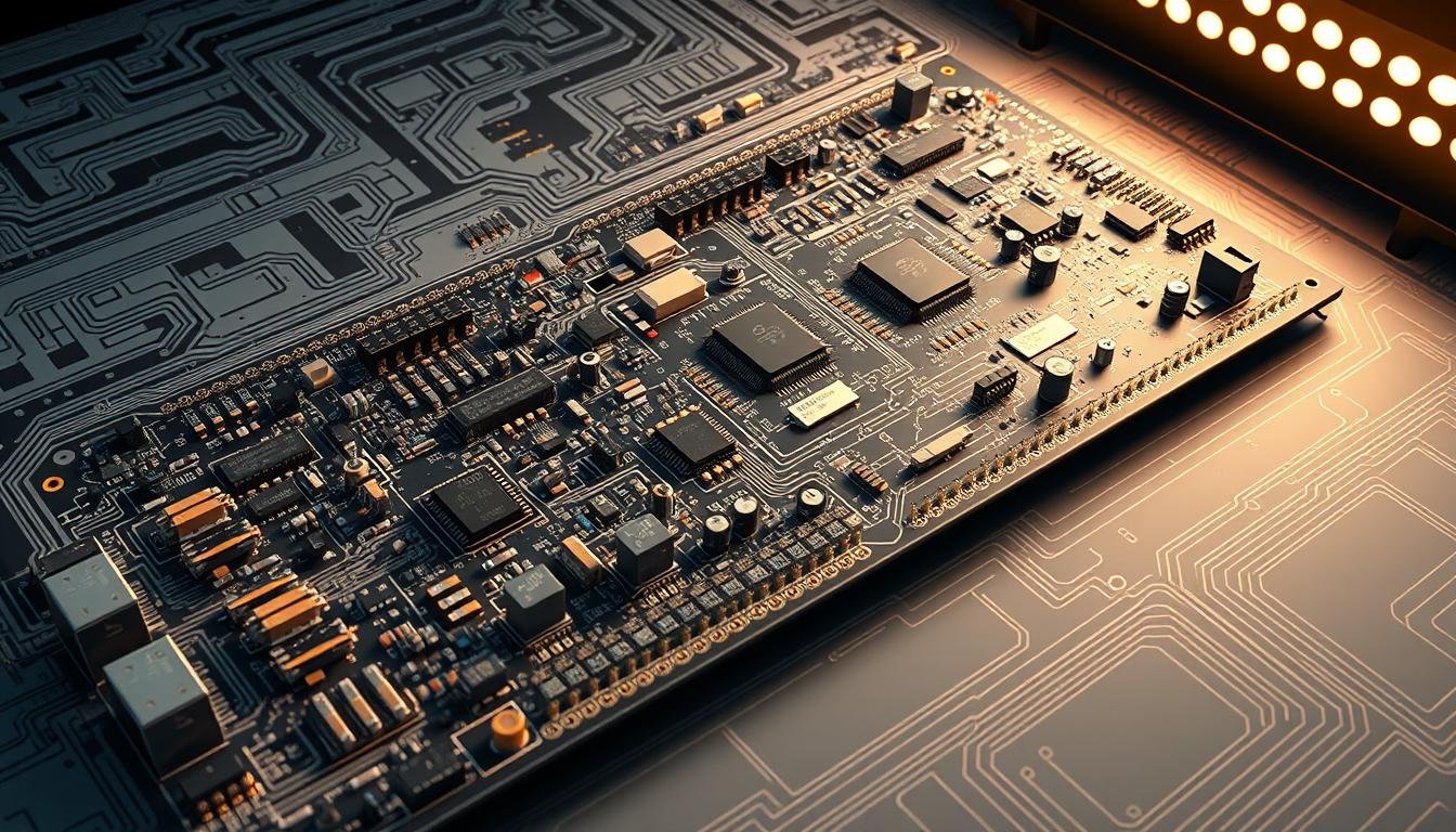
, showcasing the various electronic components in precise detail. The foreground features an array of resistors, capacitors, integrated circuits, and other surface-mount devices arranged in a logical, organized layout. The middle ground includes the PCB substrate, with its copper traces and plated-through holes clearly visible. The background depicts the assembly framework, with precise measurements, annotations, and technical specifications. The overall scene is rendered in a clean, technical style, with crisp lines, accurate proportions, and subtle lighting that highlights the intricate details of the components. The mood is one of technical precision and engineering excellence, perfectly suited to illustrate the importance of a detailed assembly drawing in the PCB manufacturing process.")
Clear documentation separates successful PCB projects from costly revisions. While fabrication drawings focus on bare board creation, assembly drawings map component integration for functional devices.
Documentation Contrasts
Fabrication and assembly drawings serve distinct purposes:
| Feature | Fabrication Drawing | Assembly Drawing |
|---|---|---|
| Primary Focus | Board layers & materials | Component positions & orientation |
| Critical Data | Drill charts, stackups | XY coordinates, BOM links |
| User Audience | Board fabricators | Assembly technicians |
Precision Manufacturing Advantages
Detailed assembly guides prevent 68% of placement errors according to IPC-7351 standards. They specify:
- Surface-mount device rotation angles
- Through-hole component insertion depths
- Mechanical part attachment sequences
Proper documentation aligns with fabrication and assembly requirements across global partners. Automated pick-and-place machines achieve 99.4% accuracy when fed precise XY data from assembly files.
Integrated bills of materials (BOM) reduce component substitution risks. They cross-reference manufacturer part numbers with placement locations, ensuring correct ICs and connectors reach their designated positions.
Creating and Utilizing Effective PCB Assembly Drawings

Precision assembly requires more than just component placement coordinates. Modern PCB documentation bridges the gap between digital designs and physical circuit boards through visual manufacturing guides. These instructions ensure every capacitor, resistor, and IC reaches its designated position with millimeter accuracy.
Step-by-Step Guide to Developing Your Assembly Documentation
Leading CAD tools offer distinct approaches for creating assembly guides. Eagle EDA exports Gerber files first, then layers drill symbols over component placements. KiCAD uses graphic tools to define board outlines and layer stackups visually.
Altium Designer streamlines the process through integrated databases. Its Draftsman module automatically links design data to fabrication notes. This eliminates manual entry errors while maintaining version control across teams.
Critical steps for reliable documentation:
- Extract component coordinates from CAD layouts
- Verify mechanical attachments in 3D viewer
- Cross-reference BOM part numbers with placement maps
Integrating Assembly Drawings with Gerber Data for Seamless Production
Consistent layer alignment prevents 73% of manufacturing discrepancies. Modern systems sync assembly files with Gerber data through:
- Automated design rule checks
- Real-time layer stackup validation
- Unified revision tracking
Advanced CAD platforms now embed assembly instructions directly into fabrication packages. This integration reduces setup time by 40% for complex printed circuit boards. Production teams receive synchronized data streams instead of disconnected file sets.
Quality assurance protocols should include automated coordinate verification and thermal stress simulations. These steps ensure components survive soldering processes while maintaining electrical performance.
Conclusion
In modern electronics manufacturing, comprehensive documentation bridges the gap between design concepts and functional products. Gerber files and assembly drawings work together like precision instruments – one defines board architecture, the other ensures component integration. This dual approach maintains design integrity across fabrication lines and assembly floors.
Our analysis confirms that complete documentation packages serve multiple critical functions. They enable clear communication between engineering teams and manufacturing partners. They create reproducible processes for current and future production cycles. Most importantly, they prevent the 37% cost overruns typically caused by incomplete specifications.
The most effective teams treat documentation as living assets. Regular updates ensure alignment with evolving industry standards and manufacturing capabilities. By combining technical accuracy with strategic foresight, organizations transform routine paperwork into competitive advantages.
Successful PCB development ultimately depends on this balance. Precise files and detailed drawings form the foundation for reliable, scalable production. They turn complex circuit designs into market-ready electronics – efficiently and predictably.