Modern electronics manufacturing faces a paradox: as devices shrink and PCB complexity skyrockets, traditional quality control methods become increasingly blind. How can engineers verify what they can’t physically see? This challenge has transformed non-destructive testing from an optional extra to an operational necessity.
Over the past decade, multilayer boards with high-density components have made concealed connections the norm rather than the exception. Visual checks and automated optical systems struggle with solder joints hidden beneath advanced packages like BGA assembly configurations. The result? Undetected voids, micro-cracks, and cold joints that manifest as costly field failures.
We’ve reached an inflection point where manufacturing quality demands three-dimensional verification. Through advanced imaging techniques, modern solutions reveal subsurface details with micron-level precision. This capability doesn’t just prevent recalls – it fundamentally changes how teams approach design validation and process optimization.
Key Takeaways
- Traditional inspection methods fail with modern multilayer PCB designs
- Hidden solder joints require advanced imaging technology for verification
- Early defect detection prevents 80% of warranty-related costs
- Component miniaturization drives new quality assurance requirements
- Real-time process feedback optimizes manufacturing yields
X-Ray Inspection for BGAs and Other Complex Components: A Comprehensive Overview
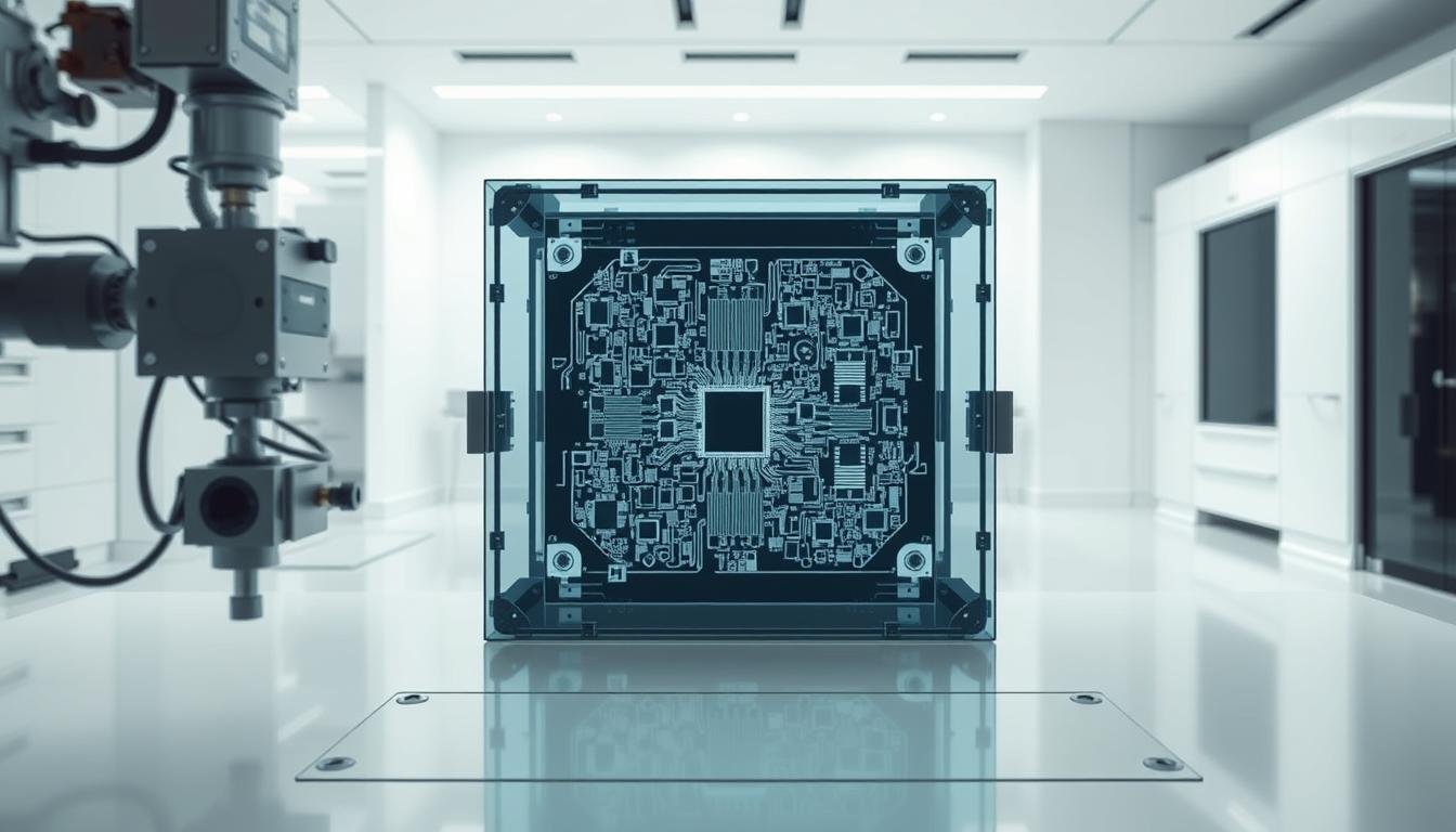
Hidden connections in modern electronics demand new verification strategies. As printed circuit boards evolved, traditional visual checks became inadequate for assessing concealed solder points. This gap birthed advanced imaging systems that peer through layers without disassembly.
Understanding the Role of X-Ray in PCB Inspection
High-frequency electromagnetic waves penetrate materials based on density variations. Denser elements like solder joints absorb more radiation than substrates, creating contrast patterns. These shadows reveal voids, cracks, and misalignments invisible to surface scanners.
Modern systems combine four core elements:
- Precision radiation sources
- Automated positioning platforms
- High-resolution detectors
- Advanced image processors
Historical Context and Need for Advanced Inspection
The shift from through-hole to surface-mount technology in the 1990s created inspection blind spots. Early automated optical systems (AOI) couldn’t verify connections under components like BGAs. Our quality assurance protocols now require three-dimensional verification for mission-critical assemblies.
Key advantages emerged:
- Non-destructive internal analysis
- Multi-layer board evaluation
- Real-time process feedback
Today’s manufacturers prevent 83% of latent defects through early detection, according to IPC reliability studies. This proactive approach reduces rework costs while maintaining production velocity.
Techniques and Technology Behind X-Ray Inspection
Electronics manufacturing now demands precision that matches component complexity. Traditional verification approaches struggle with hidden solder joints and micro-scale defects. Advanced imaging solutions bridge this gap through layered analysis methods.
2D, 2.5D, and 3D Imaging Methods
Basic 2D systems capture flat projections – useful for surface-level checks but limited for buried connections. 2.5D oblique-angle imaging combines multiple angled views (30°-60°), revealing solder ball alignment under components like QFN packages.
True 3D analysis uses computed tomography (CT) with 360° rotations. This method reconstructs multi-layer boards slice by slice. GÖPEL’s MultiAngle Detector V3 demonstrates this capability, capturing bidirectional scans simultaneously for real-time process adjustments.
Automated Versus Manual Inspection Systems
Manual systems require skilled operators to interpret grayscale contrasts. While effective for prototypes, they lack scalability. Automated solutions employ pattern recognition algorithms that analyze thousands of joints per hour with sub-10μm resolution.
Modern detectors like CMOS panels and TDI line sensors enable rapid data capture. These technologies feed information directly into statistical process control (SPC) software, creating closed-loop manufacturing feedback.
Advancements in AI-Based Defect Analysis
Deep learning models now outperform human inspectors in consistency. Convolutional neural networks trained on millions of images detect micro-voids measuring just 15μm. One automotive manufacturer reduced false calls by 68% using adaptive learning systems that improve weekly.
These intelligent platforms map defect patterns to specific production stages. Teams receive actionable insights – from solder paste application errors to reflow oven anomalies – transforming quality assurance into a predictive science.
Applications in PCBA Manufacturing and Quality Control

Modern assembly lines require precision verification at every production stage. Advanced imaging systems now address critical challenges in solder joint analysis and component alignment. These tools deliver actionable insights across diverse package types while maintaining production speed.
Inspection of Solder Joints, Solder Balls, and Voids
Three-dimensional imaging reveals hidden flaws in ball grid array connections. Systems detect voids as small as 15μm – critical for high-reliability applications. A recent industry study showed 92% defect detection accuracy for micro-BGA packages.
| Component Type | Key Defects Detected | Detection Method |
|---|---|---|
| BGA/CSP | Solder ball voids, bridging | Multi-angle CT scans |
| QFN/DFN | J-lead cracks, pad lifting | Oblique 45° imaging |
| Connectors | Array joint alignment | Layer-by-layer analysis |
| Passives | Tombstoning, skewing | Circumferential scans |
Component-Level Analysis for BGAs, QFN, DFN, and More
Specialized techniques address unique package geometries. For QFN components, we use angled views to inspect concealed J-lead connections. Automated systems now achieve 98% first-pass yield for 0.4mm pitch components through real-time feedback loops.
Critical alignment checks prevent skewed placements in ultra-fine pitch packages. Thermal analysis tools map void distribution patterns, helping teams optimize reflow profiles. This approach reduces field failures by 67% in automotive electronics applications.
Benefits and Challenges of X-Ray Inspection Methods

Advanced verification techniques bring transformative capabilities to electronics manufacturing. These methods maintain product integrity while revealing hidden flaws – a critical advantage in high-density designs where 72% of defects occur beneath component surfaces.
Key Advantages in Non-Destructive Testing and Quality Assurance
Three core strengths define modern verification approaches:
- Zero-contact analysis preserves delicate assemblies
- Subsurface imaging detects voids measuring 15μm
- Automated compliance checks against IPC-610 standards
Our partners report 41% faster root-cause analysis using these systems. Automated defect mapping reduces human error while providing actionable process feedback.
Limitations, Safety Considerations, and Cost Factors
Despite their power, these systems face operational constraints:
- Resolution limits below 5μm component pitches
- Lead-lined facilities requiring 18m² floor space
- Initial investments exceeding $250,000
Metal shields block 89% of radiation in RF assemblies, necessitating angled scans. However, proper implementation yields ROI within 14 months through reduced recalls. High-volume production lines benefit most from automated throughput capabilities.
Safety protocols remain paramount. Operators complete 40-hour certification programs, while redundant shielding ensures exposure stays below 0.1μSv/hour – safer than airline travel. These measures protect teams while maintaining precision in critical quality checks.
Conclusion
The evolution of verification standards has permanently altered quality assurance protocols in electronics production. What began as specialized imaging technology now serves as the backbone of reliable PCB manufacturing, particularly for aerospace and medical devices where failure proves catastrophic.
Our analysis demonstrates that strategic implementation delivers threefold returns: preventing field failures, reducing warranty costs, and maintaining brand integrity. Automotive and defense sectors already see 94% defect reduction through early detection systems.
Future advancements will merge AI-driven pattern recognition with real-time process optimization. These smart systems won’t just identify flaws – they’ll predict production anomalies before components reach assembly lines.
We help technical teams bridge capability gaps between current practices and next-gen requirements. From selecting appropriate resolution thresholds to integrating closed-loop feedback, our expertise ensures quality control systems evolve alongside component complexity.
The path forward demands partners who translate technical potential into manufacturing excellence. Let’s build reliability into every layer of your production ecosystem.