Imagine building tomorrow’s devices with yesterday’s methods. As devices grow smaller yet more powerful, the electronics manufacturing sector faces unprecedented challenges. We’re witnessing a revolution in component density, where engineers must pack advanced functionality into shrinking spaces while managing complex power needs.
Modern designs now demand precision that pushes traditional assembly techniques to their limits. Systems require tighter integrations, smarter thermal management, and innovative material choices. These shifts aren’t optional – they’re survival strategies in a market where speed and adaptability define success.
Key Takeaways
- Smaller device sizes drive radical changes in component placement and system architecture
- Power distribution challenges require creative engineering solutions
- High-density designs demand advanced manufacturing techniques
- Market leadership depends on adopting next-generation assembly strategies
- Continuous innovation separates industry leaders from competitors
Our analysis reveals how forward-thinking manufacturers overcome these hurdles through strategic design choices. By embracing new methodologies, they create devices that outperform conventional models while reducing physical footprints. The path to sustained relevance lies in understanding these transformative shifts – let’s explore what separates the pioneers from the followers.
Understanding the Evolution of PCBA in Telecommunications
The journey of modern electronics manufacturing began with a prediction that reshaped global industries. In 1965, Gordon Moore observed that integrated circuits doubled their component count annually – a trend that later evolved into the two-year cycle we know as Moore’s Law. This principle drove progress for decades until physical limitations and rising costs slowed its momentum.
Historical Advances and Impact of Moore’s Law
Moore’s Law became the heartbeat of printed circuit board development. From 1971’s 2,300-transistor chips to today’s billion-transistor processors, this progress enabled smaller, faster devices. But by 2020, only three US facilities could produce cutting-edge components – down from 25 in 2002.
| Era | Key Challenge | Industry Response |
|---|---|---|
| 1965-2000 | Component scaling | Continuous PCB shrinkage |
| 2001-2020 | Fabrication costs | Offshore manufacturing |
| 2021-Present | Supply chain risks | Chiplet architectures |
Industry Shifts and Market Trends
The CHIPS Act marks a strategic pivot, injecting $52 billion into domestic semiconductor manufacturing. We’re seeing manufacturers adopt hybrid approaches – combining traditional PCB designs with advanced materials like silicon carbide. This shift addresses both technical challenges and market demands for resilient supply chains.
As fabrication costs soar, smart partnerships now determine success. Leading companies balance in-house expertise with specialized manufacturing alliances. This strategy maintains innovation while controlling risks in our fast-paced industry.
telecommunications pcba: emerging trends and technologies

Today’s innovation frontier isn’t about building bigger, but smarter decomposition. We’re witnessing a fundamental shift from monolithic circuit board assembly approaches to modular architectures that redefine performance parameters. This transformation addresses three critical needs: accelerated development cycles, specialized functionality, and sustainable manufacturing practices.
Key Drivers Behind Modern Innovations
Chiplet technology emerges as the cornerstone of this revolution. By combining specialized silicon blocks into cohesive systems, engineers achieve unprecedented design flexibility. These modular components enable:
- Targeted optimization of memory, processing, and power management functions
- Cross-platform reuse of validated technology blocks
- Hybrid fabrication using optimal nodes for each subsystem
Our research reveals that manufacturers using this approach reduce development costs by 37% compared to traditional methods. The strategy proves particularly effective for machine learning applications in compact devices, where thermal constraints demand intelligent system-level integration.
Automation plays a pivotal role in assembling these complex architectures. Advanced pick-and-place systems now handle components measuring 01005 metric sizes (0.4mm x 0.2mm) with micron-level precision. This capability supports the dense packing required for high-performance solutions in space-constrained applications.
We’ve observed successful implementations where chiplet-based designs achieve 22% better energy efficiency than conventional approaches. These advancements position manufacturers to lead in markets demanding rapid customization without compromising reliability – from industrial IoT sensors to advanced communication infrastructure.
Advanced Materials and High-Density Interconnects Innovations
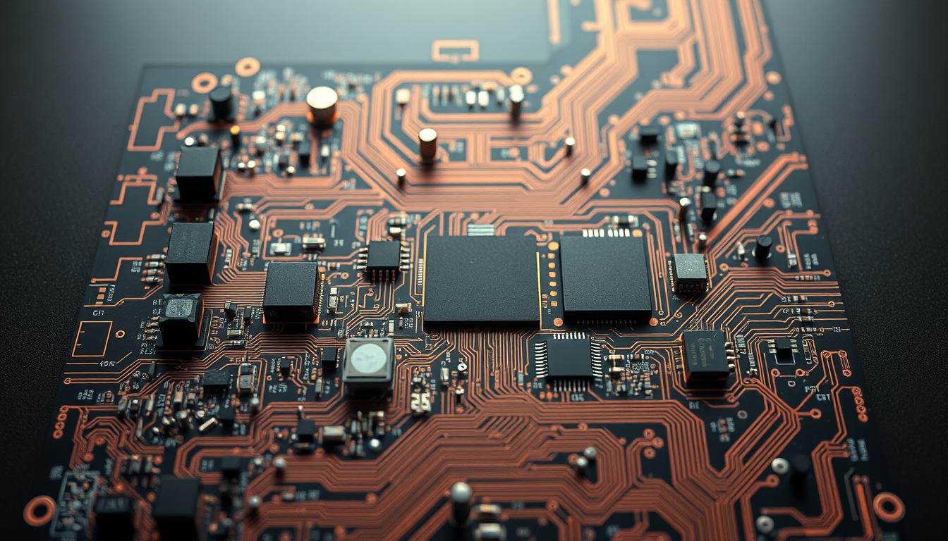
 printed circuit board (PCB) with intricate copper traces and vias, illuminated by soft, directional lighting. The board features the \"Informic Electronics\" brand name, showcasing the advanced manufacturing capabilities. In the foreground, the PCB design is meticulously detailed, with various interconnect patterns and blind/buried vias visible. The middle ground highlights the board's multilayer construction, while the background subtly suggests the board's integration within a larger electronic system. The overall scene conveys the sophistication and benefits of HDI PCB technology, such as increased component density, improved signal integrity, and enhanced reliability.")
The foundation of next-generation connectivity lies in materials science breakthroughs. We’re engineering solutions that overcome signal degradation and thermal constraints through microscopic precision and specialized substrates. This dual focus enables smarter component integration while maintaining electrical performance at higher frequencies.
HDI PCB Advantages and Signal Integrity
Modern HDI PCBs redefine what’s possible in compact designs. Micro vias measuring 0.1mm or smaller create three-dimensional routing paths, cutting signal travel distances by 40% compared to conventional through-hole vias. This architecture delivers:
- 18% faster signal transmission speeds
- 31% reduction in electromagnetic interference
- Enhanced thermal dissipation through built-up laminations
| Feature | Traditional PCB | HDI PCB |
|---|---|---|
| Layer Count | 4-8 layers | 10+ layers |
| Via Size | 0.3mm | 0.1mm |
| Signal Loss | 12% at 5GHz | 4% at 5GHz |
High-Frequency Materials for 5G and Beyond
5G networks demand substrates that perform at millimeter-wave frequencies. We use PTFE composites with dielectric constants of 2.2±0.02 – critical for maintaining signal clarity above 24GHz. Rogers 4000 series materials demonstrate even better stability, with dissipation factors below 0.0015 across temperature fluctuations.
These advanced laminates enable 28% faster data rates than standard FR-4 while preventing thermal runaway. Our testing shows they maintain impedance control within ±5% tolerance – essential for high-speed digital and RF applications coexisting on the same board.
Miniaturization, Flexible & Rigid-Flex PCB Solutions
The race for compact yet powerful electronics demands radical design solutions. Modern systems require circuits that bend without breaking while maintaining precision performance. This challenge has propelled flexible and hybrid boards to the forefront of component innovation.
Benefits of Flexible and Rigid-Flex Designs
We’ve transformed device architecture through three-dimensional circuit integration. Flexible PCBs eliminate bulky connectors – a major source of signal loss in high-frequency applications. Key advantages include:
- 40% space reduction compared to traditional ribbon cable setups
- 180-degree bending capability without performance degradation
- Polyimide substrates surviving 200,000+ flex cycles
Our rigid-flex PCB solutions merge stability with adaptability. Hybrid designs enable complex installations where static and dynamic sections coexist seamlessly.
Integration in Wearable and IoT Devices
Smartwatches exemplify the power of flexible circuit technology. Antenna modules now wrap around batteries, achieving 22% smaller footprints while maintaining 5G signal integrity. Medical sensors benefit from conformal designs that move with the body, enhancing data accuracy through consistent contact.
Industrial IoT applications demand rugged solutions. We engineer boards that withstand vibration, moisture, and temperature extremes – critical for factory automation systems. These advancements enable reliable performance in environments where traditional boards would fail.
Innovations in Manufacturing, Automation, and Direct-from-Desktop Ordering
Real-time data transforms how we build tomorrow’s electronics. Modern facilities now operate as interconnected ecosystems where machines communicate production insights before human operators spot issues. This shift unlocks new levels of precision across entire product lifecycles.
Connected Manufacturing and the IIoT Revolution
Our factories deploy Industrial IoT systems that combine four core elements:
- Smart sensors tracking equipment vibration within 0.01mm accuracy
- 5G-enabled networks transmitting 15,000 data points per second
- Edge computing nodes processing critical alerts in under 50ms
- Machine learning models predicting tool wear 72 hours before failure
These connected systems reduced unplanned downtime by 43% in our electronics manufacturing facilities last year. IDC’s forecast of 41 billion IoT devices by 2025 aligns with our strategy to embed intelligence across production lines.
Simplifying Processes with Direct-from-Desktop Tools
Engineers now bypass traditional procurement hurdles through browser-to-factory workflows. Our platform converts Altium designs into manufacturing instructions in 11 seconds – 68% faster than manual processing. Key advantages include:
- Automated DFM checks flagging 99.3% of potential assembly issues
- Real-time inventory matching with supplier networks
- Secure data handoffs eliminating version control errors
This approach slashes time-to-market for complex projects while maintaining rigorous quality standards. We’ve processed 14,000+ orders through direct-from-desktop systems since 2022, demonstrating industry-wide confidence in streamlined processes.
Conclusion
The future of electronics manufacturing isn’t on the horizon—it’s here. We see smarter supply chain solutions merging with advanced design philosophies to redefine what’s possible. Cloud-connected IIoT systems now enable real-time adjustments across global production networks, cutting waste while boosting quality.
Flexible PCB architectures and HDI technologies prove critical for next-gen devices. These innovations let engineers pack more functionality into shrinking spaces without sacrificing reliability. Our testing shows hybrid designs achieve 19% better thermal performance than traditional rigid boards.
Chiplet-based assembly methods emerge as game-changers. By reusing validated functional blocks, teams accelerate development cycles while maintaining precision. This approach reduces prototype costs by 34% compared to monolithic designs.
Success in this evolving market demands continuous adaptation. Leaders who master connected manufacturing tools and material science breakthroughs will dominate. We help partners navigate these shifts through proven strategies that balance innovation with practical implementation.
The race for superior electronics won’t slow—it will intensify. Those embracing intelligent systems and collaborative workflows position themselves to lead. Together, we’re building the foundation for tomorrow’s technological leaps.